PCB Manufacturing and Production: Processes, Quality & Efficiency
Printed circuit boards are the foundation of modern electronic products, providing both the physical platform for electronic components and the electrical connections required for circuit operation. The quality, precision, and efficiency of PCB Manufacturing directly affect the reliability, performance, development cycle, and overall competitiveness of electronic products.
Modern PCB Production is not limited to fabricating a bare circuit board. It involves a complete manufacturing workflow that can include material preparation, circuit imaging, etching, drilling, copper plating, solder mask application, surface finishing, electrical testing, component assembly, inspection, and final delivery.
For manufacturers and electronics companies, an effective PCB Manufacturing Process must balance dimensional accuracy, electrical performance, production efficiency, quality control, and delivery requirements. An integrated manufacturing approach can further simplify the transition from PCB design and fabrication to component sourcing and assembly.
PCB manufacturing is a highly technical process in which every production stage can influence the final performance of the circuit board. From selecting the appropriate substrate to completing final inspection, manufacturers must maintain strict process control to ensure that the finished PCB meets the electrical, mechanical, and reliability requirements of its intended application.
Different electronic products require different PCB structures and materials. Standard FR-4 materials are widely used for general electronic applications, while high-frequency materials may be required for RF and high-speed circuits. Metal-core boards can be selected when improved thermal management is required, while rigid-flex and flexible structures provide greater mechanical flexibility for compact electronic products.
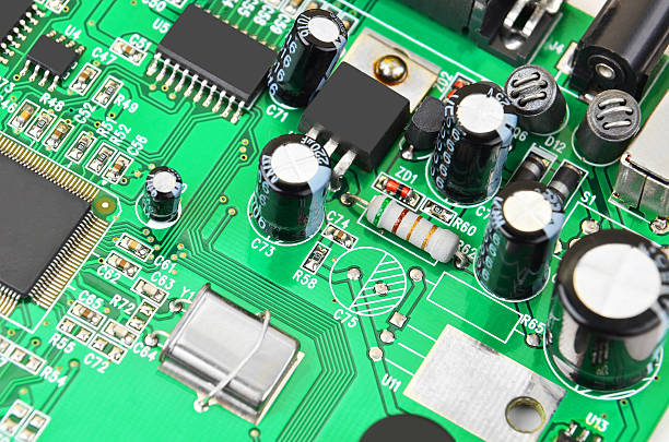
An experienced PCB manufacturer must therefore evaluate the application, layer structure, copper thickness, dielectric properties, impedance requirements, thermal conditions, and mechanical constraints before production begins.
For projects requiring complete fabrication support, PCB Manufacturing services can integrate material selection, board fabrication, inspection, and production management into a coordinated workflow. GOPCBA provides PCB fabrication and assembly services covering different PCB technologies and applications.
The substrate provides the structural foundation of a printed circuit board. Its dimensional stability, dielectric characteristics, thermal performance, and surface condition directly influence subsequent manufacturing processes.
Before circuit fabrication, PCB materials are typically cut according to the required production dimensions. The panels may then undergo cleaning and preparation to ensure that the copper surface is suitable for subsequent imaging and processing.
For high-speed or high-frequency applications, material selection becomes particularly important because dielectric properties can influence signal transmission and impedance performance. For high-power applications, thermal conductivity and heat dissipation may also become critical design considerations.
Proper material preparation helps establish the dimensional accuracy and surface quality required for the rest of the PCB Manufacturing Process.
Circuit fabrication is one of the most important stages of PCB production because it determines the conductive patterns that connect electronic components.
A typical process uses a photosensitive film and imaging system to transfer the circuit pattern onto the copper surface. The exposed material is developed to reveal the required circuit areas, after which chemical etching removes unwanted copper.
As electronic devices become smaller and more integrated, PCB designs increasingly require finer traces and tighter spacing. Manufacturing equipment must therefore provide sufficient imaging accuracy and process stability to prevent defects such as open circuits, short circuits, insufficient copper, and excessive etching.
Process parameters must be adjusted according to copper thickness, circuit density, board structure, and other design requirements.
Drilling creates the holes required for electrical and mechanical connections within a PCB. Depending on the board structure, these may include through-holes, blind vias, and buried vias.
For multilayer PCBs, drilling accuracy is especially important because the holes must align correctly with the internal copper layers. Even relatively small positional deviations can affect electrical connections and manufacturing yields.
After drilling, hole metallization creates a conductive copper layer on the hole walls. Chemical copper deposition and subsequent copper plating allow electrical connections to pass between different PCB layers.
This combination of precision drilling and reliable copper plating is fundamental to the performance of multilayer circuit boards.
While manufacturing technology determines the technical quality of a PCB, PCB Production determines how efficiently that quality can be delivered at the required volume.
PCB production involves more than operating manufacturing equipment. It requires coordinated management of customer orders, engineering data, materials, production capacity, inspection, assembly, inventory, and logistics.
A well-organized production system should be capable of handling prototype projects, small-batch orders, new product introduction, and larger production runs while maintaining consistent quality.
The production process begins with order and engineering data review. Different projects may require different manufacturing priorities.
Prototype projects often require fast engineering feedback and short production cycles. Low-volume projects may require flexible scheduling and efficient material utilization. Larger production orders require stable capacity planning, material availability, and process consistency.
Production scheduling should consider:
- PCB type and layer count
- Board dimensions
- Material requirements
- Copper thickness
- Required surface finish
- Production quantity
- Component availability
- Testing requirements
- Delivery schedule
Integrating PCB fabrication with downstream assembly can further simplify production planning. GOPCBA provides manufacturing and assembly services as part of a broader electronic manufacturing workflow.
Prototype and low-volume production are important for electronics companies developing new products. Before entering mass production, engineers need physical boards to validate electrical performance, mechanical dimensions, component placement, thermal behavior, and system functionality.
A flexible manufacturing partner can help shorten the transition from design to physical prototype.
GOPCBA offers Prototype PCB Assembly and low-volume PCB assembly services for projects that require small quantities, engineering validation, product testing, or early-stage production. Its prototype service supports PCB fabrication, component sourcing, assembly, inspection, and testing.
For low-volume requirements, the objective is not simply to manufacture fewer boards. The manufacturing process must also remain flexible enough to accommodate design revisions, component changes, and engineering feedback.
PCB fabrication produces the bare circuit board, but many electronic products require components to be installed before the board can be tested and integrated into a finished product.
This makes PCB Assembly an important part of the overall electronic manufacturing process.
Depending on the product design, assembly may include surface-mount technology, through-hole assembly, or a combination of both.
Surface-mount technology allows electronic components to be installed directly onto PCB pads. SMT is widely used because it supports high component density, compact product designs, and automated production.
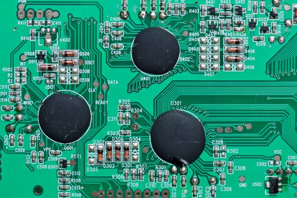
A typical SMT process includes solder paste printing, component placement, reflow soldering, inspection, and additional testing where required.
Advanced SMT manufacturing can support small components and fine-pitch devices used in increasingly compact electronic products.
Through-hole technology installs component leads through drilled holes in the PCB. It remains important for components that require strong mechanical connections or are not suitable for standard surface mounting.
Applications can include power electronics, connectors, transformers, switches, and other mechanically demanding components.
Many modern electronic products combine SMT and through-hole components. Mixed-technology assembly allows manufacturers to select the most suitable mounting method for each component.
This approach can be particularly useful for complex control boards, industrial electronics, communication equipment, power systems, and other products that combine high-density surface-mount devices with mechanically robust through-hole components.
Quality control must be implemented throughout the PCB Manufacturing Process, rather than being treated as a final inspection step.
PCB defects can originate from material problems, circuit imaging, etching, drilling, plating, solder mask application, surface finishing, assembly, or component sourcing. Detecting problems as early as possible reduces scrap, rework, and downstream failures.
Automated Optical Inspection, commonly known as AOI, uses optical systems to inspect PCB features and assembled components.
AOI can help identify problems such as:
- Missing components
- Incorrect component placement
- Solder defects
- Circuit pattern abnormalities
- Component orientation problems
- Manufacturing defects
For prototype and production projects, AOI provides an additional layer of process control and helps improve manufacturing consistency.
X-ray inspection is particularly useful for components and solder joints that cannot be fully inspected using conventional optical methods.
It can be used to evaluate hidden solder connections, including certain BGA packages, as well as internal PCB structures and other concealed features.
GOPCBA’s published prototype capabilities include AOI and X-ray inspection, along with ICT, functional testing, and other quality-control processes.
Visual inspection alone cannot verify whether an assembled PCB actually performs its intended electrical function.
Depending on the application, testing may include electrical continuity testing, insulation testing, ICT, functional testing, firmware programming, and other application-specific verification.
Testing requirements should ideally be defined before production so that the appropriate fixtures, procedures, and acceptance criteria can be prepared.
Efficient PCB Production depends on coordination between engineering, manufacturing, procurement, quality control, and logistics.
One major challenge is the separation of PCB fabrication, component sourcing, assembly, and testing among multiple suppliers. Every additional supplier can introduce another communication point and another potential source of delay.
A one-stop manufacturing model can consolidate these activities into a more coordinated workflow.
GOPCBA’s manufacturing services cover PCB fabrication, component procurement, PCB assembly, and testing, helping customers manage multiple stages of electronic production through an integrated supply chain.
Component availability can directly affect production schedules. A PCB may be fabricated on time but still be delayed if a critical integrated circuit, connector, sensor, or passive component is unavailable.
Early component sourcing can therefore help reduce production risks.
For prototype and low-volume projects, procurement is particularly important because bills of materials may contain specialized or low-availability components. Engineering teams may need to evaluate component alternatives while maintaining electrical and mechanical compatibility.
Manufacturing efficiency begins before the first PCB panel enters production.
A detailed design review can identify potential manufacturing and assembly problems before they become expensive production issues.
Typical review areas include:
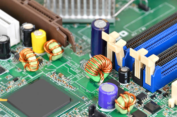
- Trace width and spacing
- Pad geometry
- Component footprints
- Component clearance
- Via dimensions
- PCB stack-up
- Impedance requirements
- Component orientation
- Assembly accessibility
- Manufacturing tolerances
GOPCBA’s PCB design and layout service includes schematic, BOM, structural information, design requirements, layout review, customer confirmation, and subsequent DFM, QA, and EMC checks.
A modern electronics manufacturing workflow can connect several stages into a continuous process:
PCB Design → Engineering Review → PCB Fabrication → Component Procurement → PCB Assembly → Inspection → Electrical Testing → Functional Validation → Delivery
This integrated approach can reduce communication gaps and make engineering changes easier to manage.
For example, a design issue discovered during prototype assembly can be communicated directly to the engineering team. The PCB layout can then be revised before the next production run.
This feedback loop is particularly valuable during new product development, where several design iterations may be required before a product is ready for volume production.
The transition from prototype to production requires more than simply increasing the quantity of boards.
Manufacturers must evaluate:
- Process repeatability
- Component availability
- Production capacity
- Assembly efficiency
- Quality standards
- Testing procedures
- Material consistency
- Production cost
- Delivery requirements
A manufacturing partner capable of supporting both prototype and production requirements can reduce the need to transfer projects between different suppliers.
GOPCBA supports PCB assembly projects from rapid prototyping and low-volume production through high-volume manufacturing, allowing customers to select a production model according to their development stage and volume requirements.
Choosing a suitable manufacturing partner is an important decision for electronics developers and purchasing teams.
An integrated supplier can provide advantages in several areas.
When PCB fabrication, component procurement, assembly, and testing are handled through separate suppliers, customers must coordinate multiple production schedules and communication channels.
A one-stop manufacturing model simplifies this workflow by placing more production stages under a single manufacturing system.
PCB projects often require technical communication regarding BOM revisions, Gerber files, component substitutions, assembly instructions, and testing requirements.
Working with an integrated engineering and manufacturing team can make these changes easier to coordinate.
When several production stages are connected, manufacturing data can be managed more consistently.
Material information, production records, inspection results, component information, and testing data can all contribute to better production traceability.
An integrated manufacturing workflow can help reduce unnecessary transportation, supplier handoffs, duplicated setup activities, and communication delays.
It can also provide a clearer view of the total production cost and delivery schedule.
PCB Manufacturing and PCB Production are comprehensive processes that combine material selection, circuit fabrication, drilling, plating, surface finishing, inspection, assembly, testing, and delivery.
The manufacturing stage determines the technical quality of the bare PCB, while effective production management ensures that products can be delivered consistently, efficiently, and according to customer requirements.
As electronic products become smaller, faster, and more complex, PCB manufacturers must provide greater precision, stronger process control, flexible production capabilities, and reliable quality assurance.
For companies developing new electronic products, working with an integrated manufacturing partner can simplify the journey from PCB design and prototype validation to low-volume production and volume manufacturing.
By combining PCB Fabrication, PCB Manufacturing, PCB Assembly, component procurement, inspection, and testing within a coordinated workflow, manufacturers can help electronics companies reduce development risks, improve production efficiency, and bring reliable products to market faster.