PCB Manufacturer: Advanced Manufacturing for Modern Electronics
As electronic products become smaller, faster, and more complex, choosing the right PCB Manufacturer has become increasingly important. PCB quality, manufacturing precision, production efficiency, and quality control can directly affect the reliability, performance, and development cycle of the final electronic product.
A professional manufacturer should offer more than basic board fabrication. Customers increasingly need a manufacturing partner that can support different development stages, from engineering review and prototype production to low-volume manufacturing and large-scale production.
An experienced supplier should also have the technical capability to manufacture different PCB structures, support specialized processes, manage demanding material requirements, and maintain consistent quality throughout production.
GOPCBA provides integrated PCB manufacturing and PCBA services designed to support electronics companies through different stages of product development and production.
What Should a Professional PCB Manufacturer Provide?
The capabilities of a professional PCB Manufacturer can generally be evaluated across four important areas: manufacturing technology, delivery flexibility, engineering support, and quality management.
A capable supplier should be able to manufacture standard PCBs as well as complex boards with high layer counts, fine traces, small vias, controlled impedance, specialized materials, and advanced interconnection structures.
At the same time, manufacturing flexibility is essential. Engineering teams may require only a small number of prototype boards during the development stage, while successful products may later require thousands or more boards for commercial production.
The ideal supplier should therefore be able to maintain manufacturing consistency while adapting production volume to the customer’s changing requirements.
Advanced PCB Fabrication Capabilities
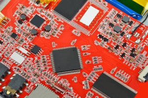
The core of PCB production is PCB Fabrication. Manufacturing capability determines whether a supplier can consistently transform a PCB design into a reliable physical product.
A comprehensive fabrication process may include material preparation, inner-layer imaging, etching, lamination, drilling, copper plating, outer-layer imaging, surface finishing, solder mask application, routing, electrical testing, and final inspection.
Different PCB structures require different process controls. Standard two-layer boards may have relatively straightforward requirements, while multilayer, HDI, high-frequency, rigid-flex, and heavy-copper boards require significantly tighter process control.
Important manufacturing parameters may include:
- Number of PCB layers
- Board thickness
- Board dimensions
- Minimum trace width and spacing
- Mechanical and laser drill sizes
- Copper thickness
- Via structure
- Controlled impedance requirements
- Surface finish
- Material type
- Solder mask and silkscreen requirements
- Special structural processes
Manufacturers must ensure that these parameters remain within the customer’s design specifications throughout the production process.
For a broader overview of available fabrication technologies, GOPCBA provides comprehensive PCB Manufacturing services covering prototype production through volume manufacturing, including multilayer, HDI, high-TG, high-speed, high-frequency, rigid-flex, heavy-copper, metal-core, and high-layer-count PCB solutions.
Multilayer PCB Manufacturing for Complex Designs
A Multilayer PCB is widely used when a circuit requires greater routing density, better power distribution, or more complex signal management.
Compared with conventional single- or double-sided boards, multilayer construction allows signal, power, and ground layers to be arranged within the internal stack-up. This helps engineers accommodate more circuitry without continuously increasing the physical size of the board.
Multilayer boards are commonly used in:
- Industrial control equipment
- Medical electronics
- Automotive electronics
- Communication systems
- Computing equipment
- Power electronics
- Networking equipment
- Consumer electronics
As layer count increases, manufacturing becomes more demanding. Layer-to-layer registration, lamination quality, dielectric thickness, copper distribution, drilling accuracy, and plating reliability all become critical.
A professional manufacturer should therefore have appropriate process controls and inspection procedures to ensure that multilayer boards maintain consistent electrical and mechanical performance.
HDI PCB for High-Density Electronic Products
The continuous miniaturization of electronic devices has increased demand for HDI PCB technology.
HDI, or High-Density Interconnect, uses advanced interconnection structures such as microvias, blind vias, buried vias, and fine-line routing to increase circuit density.
These technologies allow engineers to place more functionality into smaller PCB footprints. HDI is particularly valuable for compact electronic products where conventional through-hole structures cannot provide sufficient routing density.
Typical applications include:
- Smartphones and portable electronics
- Compact medical devices
- Automotive electronic systems
- Communication equipment
- High-density computing systems
- Industrial control products
- Consumer electronic devices
However, HDI manufacturing requires close control of laser drilling, copper plating, lamination, registration, via structures, and material selection.
For this reason, HDI designs should be reviewed carefully before production to ensure that the selected stack-up and manufacturing processes are compatible with the design requirements.
Engineering Review and Design for Manufacturing
High-quality PCB production starts with a manufacturable design.
Before fabrication begins, an engineering review can identify potential problems involving trace geometry, drill sizes, clearances, copper distribution, layer stack-up, impedance requirements, thermal management, and component placement.
Design for Manufacturing (DFM) is particularly valuable because a PCB that appears electrically correct may still create manufacturing difficulties.
For example, extremely narrow traces, insufficient spacing, unsuitable drill-to-copper clearances, complex via structures, or inappropriate material selection can increase manufacturing risks and production costs.
Early engineering analysis can help solve these issues before fabrication begins.
For customers requiring layout and engineering assistance, GOPCBA offers PCB Design/Layout services that support PCB development, DFM review, layout optimization, and manufacturing preparation.
This approach can reduce design revisions, improve first-pass production results, and create a more efficient transition from engineering prototype to production.
Specialized PCB Manufacturing Processes
Modern electronic products often require manufacturing technologies beyond standard PCB fabrication.
Heavy Copper PCB
Heavy copper technology is designed for applications that require higher current-carrying capability and improved thermal performance.
It can be useful for power electronics, industrial equipment, energy systems, automotive applications, and other products where current capacity and thermal management are important.
Resin Plugging and Via Filling
Resin plugging or via filling can improve surface flatness and support advanced component placement structures.
These technologies are often considered for high-density boards where routing and component placement requirements are particularly demanding.
Blind and Buried Vias
Blind and buried vias provide electrical connections between selected PCB layers without extending through the entire board.
They can help engineers increase routing density while reducing the space occupied by conventional through vias.
Metalized Half-Holes
Metalized half-holes can be used for certain module, edge-connection, and compact interconnection designs. Their manufacturing requires accurate routing, plating, and dimensional control.
Countersinks and Step Structures
Some mechanical and electronic products require countersunk holes, step grooves, or other customized board structures to accommodate mechanical assembly requirements.
The manufacturer should evaluate these requirements during the engineering review to ensure that the proposed process is practical and repeatable.
Surface Finishes for Different PCB Applications
Surface finishing plays an important role in solderability, corrosion resistance, electrical performance, and product reliability.
Common PCB surface finishes include:
- HASL
- Lead-free HASL
- ENIG
- OSP
- Immersion silver
- Immersion tin
- Hard gold plating
The appropriate surface finish depends on the customer’s component requirements, assembly process, environmental conditions, product lifetime, and cost considerations.
For example, ENIG is commonly considered for fine-pitch components and applications requiring a relatively flat surface, while OSP can provide a cost-effective surface protection solution for certain applications.
A professional manufacturer should be able to recommend an appropriate finish based on the actual application rather than using the same process for every board.
Quality Control Throughout PCB Manufacturing
Quality control should cover the entire manufacturing process rather than relying only on final inspection.
A robust quality management process may include incoming material inspection, engineering verification, process monitoring, in-process inspection, electrical testing, dimensional inspection, and final quality verification.
Incoming Material Inspection
Raw materials such as laminates, copper foil, solder mask materials, and other production materials should be checked against the specified requirements before entering production.
Material selection is especially important for high-frequency, high-speed, high-TG, flexible, and other specialized PCB applications.
In-Process Inspection
Critical processes such as imaging, etching, lamination, drilling, copper plating, and surface finishing require process monitoring.
Potential issues such as registration errors, insufficient copper plating, over-etching, under-etching, drilling defects, and surface abnormalities should be identified as early as possible.
Electrical Testing
Electrical testing can verify circuit continuity and isolation. Depending on the product and production requirements, testing methods may include flying probe testing or fixture-based electrical testing.
For high-speed and controlled-impedance designs, impedance testing can also be an important part of quality verification.
Dimensional and Visual Inspection
Dimensional inspection can verify board thickness, outline dimensions, hole sizes, and other mechanical characteristics.
Visual inspection can identify issues such as scratches, contamination, solder mask defects, exposed copper, surface irregularities, and other visible abnormalities.
Production Flexibility from Prototype to Volume
PCB production requirements change as products move through the development lifecycle.
During the initial development stage, engineers may need only a few prototype boards. The priority is usually fast turnaround and engineering support.
Once the design has been validated, customers may move into low-volume or small-batch production. At this stage, the manufacturer needs to balance flexibility, production efficiency, and cost.
After market validation, demand may increase significantly, requiring a stable high-volume manufacturing process.
A reliable supplier should be able to support these transitions without forcing the customer to repeatedly change manufacturing partners.
GOPCBA supports different production requirements through Prototype PCB Assembly and broader PCBA manufacturing capabilities, helping customers connect prototype development with subsequent production stages.
Integrated PCB and PCBA Manufacturing
For many electronic products, PCB fabrication is only one step in the complete manufacturing process.
After the bare PCB is manufactured, electronic components must be sourced and assembled. Depending on the product, assembly may involve SMT, through-hole technology, or a combination of different assembly technologies.
Using separate suppliers for PCB fabrication, component procurement, and assembly can create additional communication and logistics challenges.
An integrated manufacturing partner can simplify this process by coordinating multiple stages through one production workflow.
GOPCBA provides Components Procurement services as part of its broader electronics manufacturing capabilities, helping customers coordinate component sourcing with PCB assembly requirements.
For customers looking for a more comprehensive manufacturing solution, turnkey services can further integrate PCB procurement, component sourcing, assembly, inspection, testing, and delivery.
How to Choose the Right PCB Manufacturer
Selecting a PCB Manufacturer should involve more than comparing unit prices.
The right supplier should be evaluated according to the complete manufacturing requirements of the project.
1. Evaluate Manufacturing Capabilities
Check whether the manufacturer can support the required layer count, board thickness, materials, trace dimensions, via structures, surface finishes, impedance requirements, and specialized processes.
2. Review Engineering Support
A supplier with strong engineering capabilities can identify manufacturing risks before production and provide practical DFM recommendations.
3. Check Quality Control
Ask about AOI, electrical testing, dimensional inspection, impedance testing, X-ray inspection, and other quality-control procedures relevant to your PCB design.
4. Consider Production Scalability
Make sure the manufacturer can support your project from prototype and low-volume production through higher-volume manufacturing.
5. Evaluate Supply Chain Integration
For PCBA projects, component sourcing and availability can have a significant impact on delivery schedules. Integrated procurement and assembly services can simplify project management.
6. Consider Communication Efficiency
Fast and accurate communication is especially important for complex PCB projects. Engineering questions, design changes, BOM updates, and manufacturing feedback should be handled efficiently.
Why PCB Manufacturing Quality Matters
PCB quality affects much more than the appearance of a circuit board.
A manufacturing defect can result in electrical instability, intermittent connections, signal-integrity problems, assembly failures, reduced product lifetime, or even complete product failure.
As PCB designs become more complex, manufacturing precision becomes increasingly important.
For example, a small variation in trace geometry can affect controlled impedance. Poor registration can create problems in multilayer structures. Inadequate drilling or plating can compromise via reliability. Incorrect material selection can negatively affect thermal or high-frequency performance.
This is why choosing a capable PCB Manufacturer at the beginning of the project can help reduce technical and production risks later.
GOPCBA: Supporting PCB Projects from Development to Production
Modern electronics companies need manufacturing partners that can respond to both technical complexity and changing production volumes.
GOPCBA combines PCB fabrication and PCBA manufacturing capabilities to support different stages of electronic product development.
From PCB design review and prototype production to multilayer and HDI fabrication, component procurement, SMT assembly, through-hole assembly, testing, and production support, an integrated manufacturing workflow can help simplify project management.
For customers requiring complete production services, Turnkey PCB Assembly can connect multiple manufacturing stages into one coordinated process.
Conclusion
Choosing a reliable PCB Manufacturer is essential for companies developing and producing modern electronic products.
A professional supplier should have strong PCB Manufacturing capabilities, comprehensive PCB Fabrication technology, and the ability to manufacture advanced products such as Multilayer PCB and HDI PCB designs.
Beyond fabrication technology, engineering support, quality management, production flexibility, component sourcing, and assembly capabilities can also have a major impact on project success.
Whether the requirement is a prototype, a small production run, or a scalable manufacturing program, selecting a supplier with integrated capabilities can help reduce development risks, improve production efficiency, and create a more reliable path from PCB design to finished electronic products.