PCB Manufacturing Company: Comprehensive Solutions from Prototype to Production
A professional PCB Manufacturing Company is much more than a factory that produces printed circuit boards. Today, electronics manufacturers need a partner that can support different stages of product development, from initial design verification and prototype production to small-batch manufacturing and volume production.
The right manufacturing partner should combine engineering expertise, advanced fabrication capabilities, quality control, flexible production, and responsive customer service. These capabilities help electronics companies reduce development risks, improve product reliability, and move from prototype to production more efficiently.
GOPCBA provides integrated PCB fabrication and PCBA manufacturing services for a wide range of electronic applications. Its capabilities cover PCB design support, fabrication, component sourcing, PCB assembly, testing, and production services, allowing customers to manage multiple manufacturing requirements through a single supply chain.
Flexible PCB Production for Different Project Stages
One of the most important advantages of a professional PCB Manufacturer is the ability to support different production volumes.
During the research and development stage, engineers may only need a small number of boards for functional testing and design validation. At this stage, fast prototype production can help identify circuit, layout, thermal, mechanical, and assembly problems before larger investments are made.
As a product moves into pilot production, the manufacturer should be able to provide stable low-volume production without forcing customers to immediately commit to large quantities. Once the product has passed validation and enters commercial production, the same manufacturing partner should ideally be capable of scaling production while maintaining consistent quality.
This production flexibility is particularly important for startups, engineering teams, industrial equipment manufacturers, communication equipment developers, and other companies that frequently move between prototype and production stages.
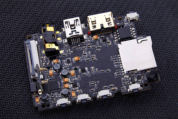
For customers who need component assembly as part of prototype development, Prototype PCB Assembly can help connect PCB fabrication with component placement, soldering, inspection, and functional verification.
Broad PCB Fabrication Capabilities for Modern Electronics
Different electronic products require different PCB structures and material systems. A capable PCB Fabrication supplier should therefore offer more than standard two-layer FR-4 boards.
Common PCB technologies include standard single- and double-sided boards, Multilayer PCB designs, high-TG PCBs, high-speed and high-frequency PCBs, HDI structures, rigid-flex PCBs, flexible PCBs, metal-core PCBs, and heavy-copper boards.
Multilayer construction is particularly useful when a circuit requires higher routing density. By adding internal signal, power, and ground layers, engineers can achieve more complex routing while maintaining a relatively compact board size.
High-frequency and high-speed applications introduce additional requirements. Material selection, impedance control, stack-up design, trace geometry, dielectric characteristics, and signal integrity all need to be considered during the design and manufacturing process.
GOPCBA’s PCB Manufacturing services cover prototype through mass production and include multilayer, HDI, high-TG, high-speed, high-frequency, rigid-flex, heavy-copper, metal-core, and high-layer-count PCB solutions.
HDI and High-Density PCB Technologies
Modern electronic devices continue to become smaller while requiring greater functionality. This trend increases the demand for HDI PCB technology.
HDI manufacturing uses high-density interconnections such as microvias, blind vias, buried vias, and other advanced structures to increase routing density. These technologies allow designers to place more electrical functions into a smaller physical area.
HDI technology is commonly considered for smartphones, compact computing systems, medical electronics, communication equipment, automotive electronics, and other products where board space is limited.
However, HDI production requires close control of laser drilling, copper plating, registration, dielectric materials, via structures, and layer alignment. Manufacturing feasibility should therefore be evaluated before production begins.
A reliable supplier can also review the stack-up and layout during the engineering stage to identify potential manufacturing risks before fabrication starts.
Engineering Review and DFM Support
PCB manufacturing quality starts before the first board enters production.
A professional engineering review evaluates whether the customer’s design can be manufactured consistently and economically. Typical review items include trace width and spacing, drill sizes, component clearances, copper distribution, layer stack-up, impedance requirements, thermal considerations, and manufacturing tolerances.
Design for Manufacturing (DFM) analysis is especially valuable for complex boards. It can identify potential problems before fabrication and help engineers modify the design while changes are still inexpensive.
For projects that require professional layout assistance, GOPCBA provides PCB Design/Layout services covering layout evaluation, stack-up considerations, component placement, routing, DFM inspection, QA review, and manufacturing documentation.
This early engineering involvement can reduce rework, improve first-pass yield, and create a smoother transition from prototype to production.
Specialized PCB Manufacturing Processes
Standard PCB production processes are sufficient for many applications, but advanced electronic products may require additional manufacturing technologies.
Depending on the design, specialized PCB processes can include:
Heavy Copper PCB
Heavy copper construction is suitable for applications requiring higher current-carrying capability and improved thermal performance. It is commonly considered for power electronics, energy systems, industrial equipment, and other high-current applications.
Resin Plugging and Via Filling
Resin plugging and via filling can improve surface flatness and support advanced structures such as via-in-pad designs. These processes are especially useful when component density and routing requirements are high.
Blind and Buried Vias
Blind and buried vias allow electrical connections between selected PCB layers without occupying space through the entire board. They can help increase routing density and reduce board size.
Controlled Impedance
High-speed digital and RF circuits require careful impedance management. Trace geometry, dielectric thickness, copper thickness, and stack-up structure all influence impedance performance.
Surface Finishes
Common surface finishes include HASL, ENIG, OSP, and other specialized finishes. The appropriate finish depends on solderability, component requirements, environmental conditions, electrical performance, and expected product life.
Quality Control Throughout PCB Production
Reliable PCB manufacturing requires quality control at multiple stages rather than relying only on final inspection.
A comprehensive production process typically includes incoming material inspection, engineering review, inner-layer inspection, imaging and etching control, lamination monitoring, drilling inspection, copper plating control, outer-layer inspection, surface finishing, electrical testing, and final inspection.
Automated Optical Inspection (AOI) can identify pattern-related defects such as opens, shorts, line-width deviations, and other abnormalities.
X-ray inspection can be useful for complex multilayer structures, hidden solder joints, microvias, and other internal features that cannot be fully evaluated through conventional visual inspection.
Electrical testing is also essential for verifying circuit continuity, isolation, and overall electrical integrity before shipment.
These inspection processes become increasingly important as board structures become more complex and component density increases.
Material Selection for Different Applications
Material selection has a direct influence on PCB electrical, thermal, mechanical, and reliability performance.
Standard FR-4 remains widely used for general electronic products. However, applications with higher thermal requirements may require high-TG materials, while high-frequency applications may require specialized materials such as Rogers.
Aluminum substrates can provide efficient thermal management for applications such as power electronics and LED systems. Flexible and rigid-flex materials are useful when a product requires bending, compact packaging, or three-dimensional interconnection.
A professional PCB Manufacturer should evaluate the material according to the electrical characteristics, operating temperature, mechanical requirements, signal frequency, reliability expectations, and production process.
From PCB Fabrication to Complete PCBA Manufacturing
For many customers, manufacturing the bare PCB is only one part of the electronics production process. Components must also be sourced, assembled, inspected, tested, and prepared for final integration.
An integrated manufacturing partner can simplify this process by connecting PCB fabrication with component procurement and PCB assembly.
GOPCBA provides Components Procurement services to support the sourcing of electronic components as part of its broader PCBA manufacturing workflow. This can help reduce coordination between multiple suppliers and improve production efficiency.
Assembly requirements can vary significantly between products. SMT assembly is suitable for high-density surface-mounted components, while through-hole assembly can provide strong mechanical connections for certain components. Some products require a combination of both technologies.
Scalable Production from Prototypes to Volume Manufacturing
A reliable manufacturing partner should be able to adapt to changing production requirements.
Prototype projects typically prioritize speed, engineering support, and design validation. Low-volume production focuses on flexibility and cost control, while high-volume production places greater emphasis on process stability, automation, material availability, production efficiency, and consistent quality.
Maintaining continuity between these stages can reduce the risks associated with changing suppliers during product development.
For customers requiring a complete manufacturing solution, Turnkey PCB Assembly can integrate component procurement, PCB fabrication, SMT and through-hole assembly, inspection, testing, packaging, and delivery into a coordinated workflow.
How to Choose the Right PCB Manufacturing Partner
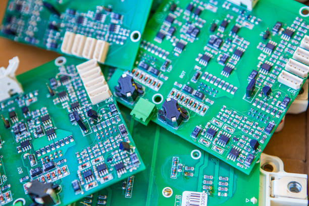
When evaluating a PCB manufacturing company, price should not be the only consideration. A lower initial quotation may not represent the lowest overall manufacturing cost if it results in repeated engineering changes, poor yields, inconsistent quality, or delayed delivery.
Consider the following factors:
1. Manufacturing Technology
Check whether the supplier can support your required layer count, materials, HDI structures, impedance requirements, copper thickness, surface finish, and other technical specifications.
2. Engineering Capability
Professional engineering support can identify DFM issues before manufacturing and help optimize the design for production.
3. Quality Control
Review the supplier’s inspection and testing procedures, including AOI, X-ray inspection, electrical testing, and final quality control.
4. Production Flexibility
Choose a supplier capable of supporting prototypes, low-volume production, and larger production requirements as your product develops.
5. Supply Chain Support
Component availability can significantly affect PCBA delivery schedules. Integrated component sourcing can simplify procurement and reduce supply-chain coordination.
6. Communication and Technical Support
Clear communication is essential when dealing with complex PCB designs. Engineering questions, BOM changes, design revisions, and production feedback should be handled efficiently.
Why Integrated PCB Manufacturing Matters
The PCB industry is moving toward increasingly integrated manufacturing services. Instead of treating PCB fabrication, component procurement, assembly, testing, and delivery as completely separate processes, electronics companies can benefit from a coordinated manufacturing workflow.
An integrated supplier can help reduce communication gaps between engineering, procurement, fabrication, and assembly teams. It can also make it easier to track design changes and resolve manufacturing issues.
For product developers, this means a smoother path from concept and prototype to pilot production and commercial manufacturing.
Conclusion
Choosing the right PCB Manufacturing Company is an important decision for any electronics product. Manufacturing capability directly affects product reliability, development speed, production cost, and long-term scalability.
A capable PCB Manufacturer should provide comprehensive PCB Fabrication capabilities, support advanced technologies such as Multilayer PCB and HDI PCB, maintain strict quality control, and provide engineering support throughout the product lifecycle.
From prototype development and design verification to low-volume production and volume manufacturing, an integrated manufacturing partner can help electronics companies reduce development risks and build a more efficient production process.
With integrated PCB fabrication, component sourcing, assembly, testing, and engineering support, GOPCBA provides a comprehensive manufacturing solution for customers developing and producing modern electronic products.