40-Layer PCB for AI Servers: Stackup Design, Signal Integrity and Thermal Management
AI servers are pushing electronic hardware toward higher computing performance, greater bandwidth, and increasingly compact system architectures. As GPUs, AI accelerators, high-speed networking devices, and power systems become more sophisticated, the PCB must provide reliable electrical connectivity while managing signal integrity, power delivery, thermal performance, and mechanical constraints.
This is one reason high-layer-count boards have become increasingly important in advanced computing platforms.
A 40-Layer PCB is not simply a conventional circuit board with more copper layers. Its stackup must be carefully engineered so that signal, power, ground, dielectric, and routing layers work together as an integrated electrical system.
For AI server applications, the PCB stackup can directly influence high-speed signal performance, power integrity, electromagnetic compatibility, thermal behavior, manufacturability, and long-term reliability.
This article explains how a 40-layer PCB can be designed and manufactured for AI server applications and the key technical factors engineers should consider.
Why AI Servers Need High-Layer-Count PCBs
AI servers process enormous volumes of data and connect high-performance processors, memory, storage, networking interfaces, and power-management circuits.
These systems create several PCB design challenges.
Increasing Signal Density
Modern AI processors and networking devices may require a large number of high-speed signal connections.
A conventional two-layer or four-layer board may not provide enough routing space for these connections.
Increasing the number of PCB layers allows designers to distribute signals across multiple routing layers while maintaining appropriate spacing and reference-plane structures.
This makes a high-layer-count Multilayer PCB particularly useful for complex computing platforms.
High-Speed Data Transmission
AI servers depend on high-speed interfaces between processors, accelerators, memory, switches, and other components.
As signaling speeds increase, PCB design becomes increasingly sensitive to:
- Insertion loss
- Return loss
- Crosstalk
- Impedance discontinuities
- Via transitions
- Dielectric loss
- Copper roughness
- Reference-plane discontinuities
- Power-supply noise
A properly designed High-Speed PCB must therefore control the complete signal path rather than focusing only on trace width.
Increasing Power Density
AI processors and accelerators can consume substantial electrical power.
The PCB must distribute high currents while maintaining stable voltage levels and minimizing power-distribution noise.
This requires careful planning of power planes, ground planes, copper thickness, current paths, vias, and decoupling structures.
Thermal Challenges
Higher computing performance also means greater heat generation.
The PCB must work with the system’s heat sink, cold plate, airflow, thermal interface materials, and mechanical structure to provide an effective thermal path.
As a result, electrical and thermal design can no longer be considered completely separate.
What Is a 40-Layer PCB?
A 40-layer PCB contains multiple conductive copper layers separated by dielectric materials.
The exact stackup varies according to the application. A typical high-layer-count board may contain a combination of:
- High-speed signal layers
- General signal-routing layers
- Ground planes
- Power planes
- Low-speed control layers
- Auxiliary routing layers
Not every layer needs to perform the same function.
The purpose of the stackup is to create a controlled electrical environment in which high-speed signals have appropriate reference planes, power distribution remains stable, and routing density can be accommodated within the available board area.
Therefore, simply increasing layer count does not automatically improve PCB performance.
Stackup architecture is more important than layer count alone.
Typical Structure of a 40-Layer AI Server PCB
There is no universal 40-layer stackup for every AI server. The correct configuration depends on the processor, interface standards, board dimensions, materials, power requirements, and mechanical architecture.
A conceptual structure may include:
- High-speed signal layers
- Ground reference planes
- Additional high-speed signal layers
- Power distribution planes
- General-purpose routing layers
- Additional ground planes
- Power and control layers
- High-speed interface layers
- Ground and power reference layers
- Additional routing layers
This pattern can be repeated and optimized throughout the stackup.
The objective is to maintain appropriate signal-reference relationships and minimize unnecessary transitions.
For example, a high-speed differential pair should ideally have a stable reference plane and a controlled impedance throughout its route.
Signal Layers, Power Layers and Ground Layers
The three major functional categories in a complex PCB stackup are signal, power, and ground.
Signal Layers
Signal layers carry electrical connections between components.
High-speed signals require careful control of:
- Trace geometry
- Differential-pair spacing
- Reference planes
- Layer transitions
- Via structures
- Trace length
- Electrical skew
Low-speed signals generally have less demanding requirements, so they can often be routed on different layers.
Separating different signal groups can also reduce interference between sensitive interfaces.
Power Layers
Power planes distribute voltage and current to processors, memory devices, networking components, and other circuits.
A multilayer power structure can help reduce current-path resistance and inductance while supporting multiple voltage domains.
Power integrity depends not only on copper area but also on:
- Plane geometry
- Via distribution
- Decoupling capacitors
- Current density
- Plane resonance
- Return-path design
Ground Layers
Ground planes provide low-impedance return paths for signals and help establish stable electromagnetic reference structures.
A continuous ground plane can reduce unnecessary return-path discontinuities and help control electromagnetic coupling.
In high-speed designs, the relationship between signal traces and their reference planes is particularly important.
How Layer Count Helps High-Speed Routing
One of the primary advantages of a 40-layer structure is routing capacity.
Consider a large AI processor with hundreds or thousands of electrical connections. Routing all these connections while maintaining signal-integrity requirements can be extremely difficult with a low-layer-count board.
Additional layers provide more routing channels.
Instead of forcing many signals into the same physical region, engineers can distribute them across multiple layers.
This helps:
- Reduce routing congestion
- Improve spacing
- Maintain reference planes
- Separate sensitive interfaces
- Reduce unnecessary vias
- Simplify power distribution
- Support complex component escape routing
However, additional layers also increase manufacturing complexity, board thickness, lamination requirements, and cost.
The layer count should therefore be determined by electrical and mechanical requirements rather than used as a performance target by itself.
Signal Integrity in 40-Layer AI Server PCBs
Signal integrity is one of the most important design considerations for AI server boards.
At high data rates, a PCB trace behaves as a transmission line rather than simply as a piece of copper.
Controlled Impedance
High-speed interfaces require carefully controlled impedance.
Impedance depends on factors such as:
- Trace width
- Copper thickness
- Dielectric thickness
- Dielectric constant
- Reference-plane distance
- Manufacturing tolerances
The stackup must therefore be designed before routing begins.
Manufacturing capability is equally important because the actual fabricated dimensions must remain within the specified tolerance.
Crosstalk Control
When high-speed traces are routed too closely together, electromagnetic coupling can cause crosstalk.
Designers can reduce crosstalk through:
- Appropriate trace spacing
- Ground reference planes
- Layer separation
- Careful routing direction
- Differential-pair management
- Avoiding long parallel runs
A 40-layer architecture provides additional opportunities to separate sensitive signal groups.
Via and Layer Transitions
Vias introduce discontinuities into high-speed signal paths.
Large or poorly designed via structures can create parasitic capacitance and inductance, affecting signal quality.
For high-speed AI server boards, engineers may need to optimize:
- Via diameter
- Anti-pad size
- Via stub length
- Back-drilling requirements
- Layer transitions
- Return-via placement
These details become increasingly important as signaling speeds increase.
Power Integrity in High-Layer-Count PCBs
AI accelerators can create rapidly changing current demands.
The PCB power-delivery network must respond to these transient loads while maintaining stable voltage at the device.
A high-layer-count board can provide dedicated power and ground structures that support better current distribution.
Important design considerations include:
- Plane impedance
- Power-path inductance
- Copper thickness
- Via arrays
- Decoupling capacitor placement
- Voltage-domain separation
- Return-current paths
Power integrity and signal integrity are closely connected.
Noise on the power-distribution network can couple into sensitive signal paths, while high-speed signal activity can also affect the power system.
Thermal Management in 40-Layer PCBs
Thermal management becomes increasingly important as AI computing density increases.
A PCB itself does not replace the server’s primary cooling system, but its material structure and copper distribution can contribute to heat spreading and thermal conduction.
Potential approaches include:
Thick Copper
Higher copper weight can improve current-carrying capability and contribute to thermal spreading in appropriate areas.
Thermal Vias
Arrays of thermal vias can transfer heat between copper layers and toward a heat-spreading structure.
Copper Planes
Large copper areas can distribute heat away from localized hot spots.
Thermally Optimized Materials
The laminate system should be selected according to the required electrical, thermal, mechanical, and reliability characteristics.
Integration With External Cooling
PCB thermal design must ultimately work together with the system-level cooling solution.
For AI servers, this may include heat sinks, cold plates, airflow systems, or other thermal-management technologies.
The most effective solution is therefore a system-level approach rather than relying on the PCB alone.
Materials for AI Server PCBs
Material selection becomes increasingly important as signal frequencies and data rates rise.
Standard FR-4 materials may be suitable for many applications, but advanced high-speed designs may require materials with improved electrical properties.
Important material characteristics include:
- Dielectric constant
- Dissipation factor
- Thermal stability
- Moisture resistance
- Dimensional stability
- Glass-transition temperature
- Copper adhesion
- Low-loss performance
For high-speed channels, dielectric loss can contribute significantly to insertion loss.
Therefore, material selection should be based on the complete channel-performance requirement rather than simply choosing the lowest-cost laminate.
Manufacturing Challenges of 40-Layer PCBs
High-layer-count PCB production is considerably more complex than standard multilayer manufacturing.
The manufacturing process may involve:
- Inner-layer imaging
- Circuit etching
- Inner-layer inspection
- Layer alignment
- Lamination
- Mechanical drilling
- Laser drilling where required
- Desmear
- Electroless copper deposition
- Electrolytic copper plating
- Outer-layer imaging
- Circuit formation
- Solder mask
- Surface finishing
- Electrical testing
- Final inspection
Every additional manufacturing stage introduces potential process variation.
For this reason, advanced PCB Manufacturing requires strong control over material handling, layer registration, lamination, drilling, plating, imaging, and inspection.
GOPCBA provides advanced PCB Manufacturing solutions for complex PCB structures, including multilayer and high-density board technologies.
Why Layer Registration Is Critical
When dozens of layers are laminated together, even small registration errors can affect the relationship between traces, pads, vias, and reference planes.
This is especially important for:
- Small vias
- Fine-pitch components
- Microvias
- Blind vias
- High-density routing
- Via-in-pad structures
Manufacturers therefore need precise alignment and process control throughout multilayer fabrication.
The challenge becomes even greater when the PCB combines high layer count with fine-line routing and advanced via structures.
HDI Technology and AI Server PCBs
Some advanced AI computing boards may incorporate HDI techniques to improve routing density.
An HDI PCB can use:
- Microvias
- Blind vias
- Buried vias
- Fine traces
- Fine spaces
- Sequential lamination
- Via-in-pad structures
HDI technology can help shorten interconnects and provide more efficient escape routing around high-density components.
However, HDI does not automatically replace conventional through-hole structures. The appropriate technology depends on the board architecture and electrical requirements.
For high-density computing applications, HDI and conventional multilayer technologies may be combined as part of a customized stackup strategy.
Testing and Quality Control
A high-layer-count PCB requires comprehensive inspection because defects hidden inside the board may not be visible during final visual inspection.
Depending on the design, manufacturers may use:
- Automated optical inspection (AOI)
- Electrical continuity testing
- Isolation testing
- X-ray inspection
- Microsection analysis
- Impedance testing
- Dimensional inspection
- Surface-finish inspection
Electrical testing is especially important for verifying opens and shorts.
For controlled-impedance designs, impedance verification can also help confirm that the fabricated PCB matches the intended stackup and trace geometry.
Quality control should begin with incoming materials and continue throughout fabrication rather than being limited to final inspection.
How to Design a Reliable 40-Layer PCB
A successful 40-layer design requires cooperation between PCB designers, signal-integrity engineers, power engineers, thermal engineers, and the PCB manufacturer.
A practical workflow includes:
Step 1: Define System Requirements
Determine:
- Data rates
- Interface types
- Power requirements
- Board dimensions
- Component density
- Thermal requirements
- Reliability requirements
Step 2: Develop the Stackup
Assign signal, power, and ground layers according to electrical requirements.
Step 3: Select Materials
Choose laminate materials based on signal-loss, thermal, mechanical, and reliability requirements.
Step 4: Simulate Critical Signals
Analyze high-speed channels before manufacturing.
Step 5: Optimize Power Distribution
Evaluate voltage-drop, current density, plane impedance, and decoupling.
Step 6: Review Manufacturability
Work with the manufacturer to verify that the stackup, trace geometry, vias, materials, and tolerances are manufacturable.
Step 7: Prototype and Validate
Fabricate prototype boards and verify electrical, thermal, and mechanical performance before volume production.
Choosing a PCB Manufacturer for AI Server Boards
Not every supplier is suitable for high-layer-count AI server PCB production.
When evaluating a PCB Manufacturer, consider:
- High-layer-count manufacturing experience
- High-speed PCB capability
- Controlled-impedance manufacturing
- Advanced laminate compatibility
- Fine-line processing
- Mechanical and laser drilling
- HDI capability
- Lamination control
- Layer-registration accuracy
- Electrical testing
- Quality certifications
- Engineering support
It is also important to evaluate whether the manufacturer can provide DFM feedback before production.
For complex AI hardware, the manufacturer’s engineering team should be able to identify manufacturing risks before the board enters mass production.
From PCB Manufacturing to PCB Assembly
Bare-board manufacturing is only one stage of AI server hardware production.
After fabrication, the PCB may need to be assembled with processors, memory devices, power-management components, connectors, and other components.
Advanced assembly may involve:
- SMT placement
- Fine-pitch component assembly
- BGA assembly
- Through-hole assembly
- AOI
- X-ray inspection
- Reflow soldering
- Electrical testing
- Functional testing
Using a manufacturing partner that can coordinate PCB fabrication and assembly can simplify the supply chain and reduce communication gaps.
For projects that require an integrated production process, GOPCBA also provides PCB Assembly services covering different assembly technologies and manufacturing requirements.
The Future of AI Server PCB Technology
AI hardware continues to evolve rapidly.
Future PCB development is likely to focus on several areas:
Lower-Loss Materials
As data rates increase, lower-loss dielectric materials will become increasingly important for maintaining channel performance.
Higher Routing Density
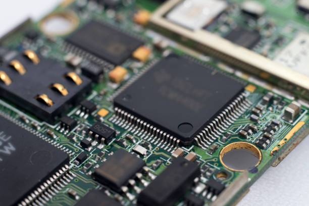
Advanced packaging and increasingly complex processors will continue to increase PCB interconnect density.
Advanced HDI
Microvia structures and sequential lamination may become increasingly important for compact, high-density computing platforms.
Better Thermal Integration
Electrical and thermal design will become increasingly interconnected as power density rises.
Advanced Manufacturing
PCB manufacturers will need greater control over dimensional tolerances, layer registration, materials, copper structures, drilling, and inspection.
Conclusion
A 40-Layer PCB can provide the routing capacity and electrical architecture required by demanding AI server platforms, but simply increasing the number of layers does not guarantee better performance.
The real challenge is designing an optimized stackup in which high-speed signals, power distribution, ground references, thermal paths, materials, and manufacturing processes work together.
For AI server applications, engineers should pay particular attention to signal integrity, impedance control, power integrity, layer registration, material selection, via structures, thermal management, and manufacturing quality.
As AI processors become more powerful and system bandwidth continues to increase, advanced Multilayer PCB technology will remain an important part of the hardware infrastructure supporting next-generation computing.