High-Frequency Hybrid PCB Lamination: Process Comparison and Material Selection
High-frequency electronic systems increasingly combine different PCB materials to meet demanding electrical, thermal, mechanical, and cost requirements. Instead of manufacturing an entire board from a single laminate system, engineers may use a hybrid PCB construction that combines conventional FR-4 with low-loss, high-frequency, PTFE-based, ceramic-filled, or other specialty materials.
This approach can provide an effective balance between electrical performance and manufacturing cost. However, combining materials with different thermal, mechanical, and dielectric characteristics creates additional manufacturing challenges.
Among all fabrication processes, PCB lamination is one of the most important factors affecting the structural integrity and electrical performance of a high-frequency hybrid PCB. Material compatibility, resin flow, dielectric thickness, thermal expansion, registration, pressure, and temperature must all be carefully controlled.
The appropriate lamination strategy depends on the material combination, layer count, electrical requirements, board thickness, production volume, and reliability requirements. This article compares major lamination approaches and explains how manufacturers can select an appropriate process for high-frequency hybrid PCB production.
What Is a High-Frequency Hybrid PCB?
A high-frequency hybrid PCB combines two or more PCB material systems within the same multilayer construction.
A typical example may combine:
- FR-4 for cost-effective structural layers
- High-speed laminate for controlled-impedance digital signals
- PTFE-based material for RF circuits
- Ceramic-filled laminate for specialized high-frequency applications
- Copper or metal structures for thermal management
- Flexible materials for mechanically constrained sections
The purpose is not simply to combine different materials. The stackup must be engineered so that the electrical, thermal, mechanical, and manufacturing characteristics of those materials remain compatible.
For high-speed and RF applications, designers may need to control:
- Dielectric constant (Dk)
- Dissipation factor (Df)
- Controlled impedance
- Dielectric thickness
- Copper roughness
- Thermal expansion
- Moisture absorption
- Z-axis expansion
- Interlayer bonding
- Registration accuracy
This makes hybrid PCB fabrication substantially more demanding than conventional multilayer PCB production.
For projects requiring advanced multilayer structures, a dedicated PCB manufacturing service should be evaluated based on material capability, stackup engineering, lamination control, and inspection resources rather than board price alone.
Why Is Lamination Critical for High-Frequency Hybrid PCBs?
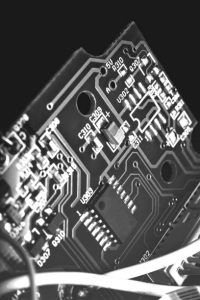
Lamination bonds copper layers, cores, and prepreg materials into a mechanically stable multilayer structure. At the same time, the lamination process determines the final dielectric construction that directly influences electrical performance.
For hybrid PCBs, this becomes more complicated because different materials may have significantly different:
- Coefficients of thermal expansion (CTE)
- Glass transition behavior
- Melting or softening characteristics
- Resin systems
- Thermal conductivity
- Dimensional stability
- Moisture absorption
- Surface characteristics
If the lamination process is poorly matched to the material system, defects can include:
- Delamination
- Voids
- Resin starvation
- Excessive resin squeeze-out
- Warpage
- Layer misregistration
- Internal stress
- Cracking
- Unstable dielectric thickness
From an electrical perspective, variations in dielectric thickness or material properties can also affect controlled impedance and signal loss.
Therefore, lamination should be considered part of the electrical engineering process, not merely a mechanical bonding operation.
Three Major Lamination Approaches for Hybrid PCBs
There is no single lamination process that is optimal for every high-frequency hybrid PCB. Three commonly considered approaches are conventional thermal lamination, vacuum-assisted lamination, and sequential or staged lamination.
Each approach has a different balance of manufacturing complexity, material compatibility, process control, and cost.
1. Conventional Thermal Lamination
Conventional thermal lamination uses controlled temperature and pressure to consolidate the multilayer stack and cure the bonding materials.
The general process includes:
- Preparing the inner-layer circuitry
- Cleaning and treating the bonding surfaces
- Stacking cores and prepreg according to the approved stackup
- Applying heat and pressure
- Allowing resin to flow and fill the required areas
- Completing the curing cycle
- Controlled cooling
- Removing the laminated panel for subsequent processing
Advantages
Conventional lamination is a mature and widely used manufacturing method. When the selected materials have compatible processing windows, it can provide:
- Good production efficiency
- Relatively straightforward process control
- Lower equipment requirements
- Stable repeatability
- Good suitability for conventional multilayer structures
It can be an appropriate solution when the hybrid material combination has relatively compatible thermal and mechanical characteristics.
Limitations
The main challenge is material compatibility.
If two materials respond very differently to temperature and pressure, applying a common lamination profile can increase internal stress or dimensional instability.
Potential issues include:
- Warpage
- Registration problems
- Inconsistent resin flow
- Voids
- Delamination
- Localized stress
Therefore, conventional thermal lamination should not be selected simply because it is familiar or inexpensive. The actual material datasheets and stackup construction need to be evaluated first.
Typical Applications
Conventional lamination can be suitable for hybrid multilayer PCBs where:
- Material combinations are relatively compatible
- Layer count is moderate
- Electrical requirements are well defined
- Production volume justifies a standardized process
- Cost efficiency is an important consideration
2. Vacuum-Assisted Lamination
Vacuum-assisted lamination introduces controlled vacuum conditions during the lamination cycle to reduce trapped air and improve consolidation of the multilayer stack.
This is particularly useful when the PCB construction contains challenging geometries, materials, or structures where conventional processing may increase the risk of internal voids.
How Vacuum Lamination Works
A typical process may include:
- Preparing and stacking the multilayer structure
- Loading the stack into the lamination system
- Establishing the required vacuum condition
- Applying a controlled heating profile
- Increasing pressure according to the process recipe
- Allowing resin to flow and cure
- Maintaining appropriate process conditions during cooling
- Removing and inspecting the laminated panel
The exact temperature, pressure, vacuum level, and timing must be determined by the material system. There is no universal vacuum-lamination profile suitable for every high-frequency laminate.
Advantages
Vacuum-assisted lamination can help reduce the risk of trapped air and improve consistency in demanding multilayer structures.
Potential benefits include:
- Improved void control
- More consistent consolidation
- Better process control for complex constructions
- Reduced risk associated with trapped air
- Improved repeatability for demanding multilayer assemblies
For high-frequency boards, reducing internal voids is particularly important because unexpected variations in the dielectric structure can influence electrical behavior.
Limitations
Vacuum systems generally require more specialized equipment and process control than basic thermal presses.
Manufacturers also need to manage:
- Vacuum-system integrity
- Material-specific heating profiles
- Resin flow
- Pressure transitions
- Cooling rates
- Panel dimensional stability
Vacuum alone does not eliminate all problems associated with incompatible materials. If two laminates have substantially different thermal expansion behavior, the underlying stackup design and material selection still need to address that mismatch.
Typical Applications
Vacuum-assisted lamination may be appropriate for:
- High-frequency multilayer PCBs
- Complex hybrid stackups
- High-reliability communication hardware
- RF and microwave applications
- Boards where void control is particularly important
- Advanced multilayer constructions
3. Sequential or Staged Lamination
Sequential lamination takes a different approach by constructing portions of the PCB in separate lamination stages.
Rather than attempting to consolidate the entire material system in one cycle, the manufacturer builds defined substructures and subsequently combines them through additional processing.
This method can be particularly useful when a PCB contains complex interconnect structures or material combinations that cannot be effectively processed using a single lamination cycle.
Basic Process Concept
A simplified sequential lamination workflow may involve:
- Manufacturing an initial subassembly
- Completing the required drilling or interconnection processes
- Preparing additional dielectric and copper layers
- Performing a second lamination cycle
- Completing subsequent drilling and metallization
- Continuing the build-up process until the final stackup is completed
The actual process varies considerably depending on whether the design uses sequential build-up, buried vias, HDI structures, mixed materials, or specialty laminates.
Advantages
Sequential lamination provides greater flexibility in complex multilayer construction.
It can help manufacturers manage:
- Different material systems
- Complex via structures
- HDI configurations
- Buried interconnects
- Fine-pitch routing
- Specialized RF sections
Because each lamination stage can be engineered around a particular substructure, manufacturers have more opportunities to control dimensional stability and registration.
Limitations
The additional process stages increase:
- Manufacturing time
- Engineering complexity
- Registration requirements
- Process-control requirements
- Cost
Sequential lamination should therefore be used when the design requirements justify its additional complexity.
High-Frequency Hybrid PCB Lamination Comparison
The three approaches can be summarized as follows:
| Factor | Conventional Thermal Lamination | Vacuum-Assisted Lamination | Sequential/Staged Lamination |
|---|---|---|---|
| Process complexity | Low to moderate | Moderate | High |
| Equipment requirements | Standard | Specialized | Specialized |
| Void control | Process dependent | Stronger potential | Process dependent |
| Material compatibility | Best for compatible systems | Better process control for complex structures | High flexibility |
| Production efficiency | Generally high | Moderate | Lower |
| Cost | Lower | Moderate to high | Higher |
| Complex multilayer structures | Moderate | High | Very high |
| Best use case | Compatible material combinations | Demanding hybrid structures | Complex staged constructions |
This table should be treated as a general engineering comparison rather than a universal ranking. Actual results depend on laminate selection, stackup design, equipment, process recipe, and manufacturing controls.
How Material Compatibility Affects Lamination
Material compatibility is one of the most important considerations when developing a hybrid PCB stackup.
CTE Differences
Different materials expand at different rates as temperature changes.
The coefficient of thermal expansion is especially important in the Z-axis because repeated thermal cycles can place stress on plated through-holes and interlayer connections.
If materials with significantly different CTE characteristics are combined without proper stackup and process engineering, thermal stress can increase the risk of reliability problems.
Tg and Processing Temperature
Glass transition temperature, decomposition behavior, resin characteristics, and recommended processing conditions vary between material systems.
The lamination profile therefore needs to remain within the appropriate processing window for the materials being used.
Resin Flow
Prepreg resin flow determines how effectively the material fills spaces and bonds the multilayer stack.
Too much resin flow can change dielectric thickness and potentially affect impedance. Too little flow can result in inadequate bonding or voids.
For controlled-impedance applications, resin selection and flow behavior must be considered alongside the electrical stackup.
Dielectric Thickness and Signal Integrity
For high-frequency hybrid PCBs, the dielectric layer is part of the transmission-line structure.
A change in dielectric thickness changes the relationship between the signal trace and its reference plane. As a result, the finished impedance can differ from the value predicted during design.
This means that lamination control directly supports signal integrity.
Important parameters include:
- Final dielectric thickness
- Material Dk
- Resin content
- Copper thickness
- Trace width
- Reference-plane spacing
- Material uniformity
The manufacturer should therefore validate the actual stackup rather than relying only on nominal laminate thickness.
How to Control Lamination Quality
A robust high-frequency PCB manufacturing process should include several levels of control.
1. Material Verification
Before production, verify:
- Material type
- Material thickness
- Copper thickness
- Resin system
- Dk/Df data
- Lot information
- Supplier documentation
Material traceability is especially important for high-reliability RF and communication products.
2. Stackup Verification
The manufacturing engineering team should confirm:
- Layer sequence
- Core thickness
- Prepreg construction
- Copper distribution
- Finished board thickness
- Controlled-impedance requirements
- Via structures
- Lamination sequence
Any changes to the approved material system should undergo engineering review.
3. Lamination Profile Control
The production process should control:
- Temperature ramp rate
- Pressure
- Vacuum where applicable
- Resin flow
- Cure time
- Cooling rate
The process should be established according to the material manufacturer’s recommendations and validated for the actual stackup.
4. Dimensional and Visual Inspection
After lamination, manufacturers can inspect the panel for:
- Warpage
- Delamination
- Voids
- Surface abnormalities
- Thickness variation
- Registration issues
Additional cross-sectional analysis can be performed when required.
5. Electrical Verification
For controlled-impedance designs, electrical testing can be performed using appropriate test coupons and measurement methods.
Depending on the application, manufacturers may evaluate:
- Characteristic impedance
- Insertion loss
- Return loss
- Continuity
- Isolation
- Other application-specific electrical parameters
DFM and Engineering Review Before Production
The success of a hybrid PCB begins before the first production panel enters the lamination press.
A comprehensive engineering review should evaluate the relationship between the PCB design and the manufacturer’s actual process capabilities.
Important considerations include:
- Material availability
- Laminate compatibility
- Stackup feasibility
- Resin flow
- Copper distribution
- Thermal expansion
- Drillability
- Registration
- Controlled impedance
- Surface finish
- Expected production volume
For projects involving complex stackups, early PCB design and layout engineering can help identify manufacturability and signal-integrity risks before fabrication.
Prototype Validation Before Mass Production
Hybrid high-frequency PCBs should ideally undergo prototype validation before volume production.
A prototype can be used to verify:
- Lamination quality
- Finished dielectric thickness
- Controlled impedance
- Signal integrity
- RF performance
- Thermal behavior
- Mechanical stability
- Assembly compatibility
If the prototype reveals excessive loss, impedance deviation, warpage, or reliability concerns, the stackup and lamination recipe can be adjusted before production quantities increase.
For projects requiring assembled prototypes, prototype PCB assembly can help validate the complete electronic system rather than evaluating the bare PCB alone.
How to Select the Right Lamination Process
The best lamination method depends on several variables rather than one specification.
Choose Conventional Lamination When:
- Materials have compatible processing characteristics
- The stackup is relatively straightforward
- Production efficiency is important
- Electrical requirements can be achieved through standard process control
Consider Vacuum-Assisted Lamination When:
- Void control is especially important
- The stackup is complex
- High-frequency electrical performance is demanding
- The material system benefits from controlled consolidation
Consider Sequential Lamination When:
- The PCB requires complex multilayer structures
- Multiple build-up stages are necessary
- HDI or buried interconnect structures are involved
- Different sections of the PCB require specialized processing
In some advanced manufacturing programs, these methods can also be combined. The final process should be selected based on engineering validation rather than a generic process preference.
Cost Considerations for Hybrid PCB Lamination
Lamination represents only one portion of the total cost of a high-frequency hybrid PCB.
Other major cost drivers include:
- Specialty laminate materials
- Layer count
- Copper thickness
- HDI or sequential structures
- Drilling requirements
- Controlled-impedance tolerances
- Surface finish
- Electrical testing
- Prototype quantity
- Production volume
A low-cost lamination process may not provide the lowest total project cost if it creates poor yield or requires repeated redesigns.
For high-performance communication hardware, manufacturing yield and long-term reliability should therefore be considered together with the initial PCB quotation.
What Should Engineers Ask a PCB Manufacturer?
Before selecting a supplier for a high-frequency hybrid PCB, ask:
- Can the manufacturer process the specific laminate combination?
- Does the engineering team have experience with hybrid stackups?
- Can the manufacturer support controlled impedance?
- How are resin flow and dielectric thickness controlled?
- What lamination equipment is available?
- Can vacuum-assisted or sequential processes be supported when required?
- How is layer-to-layer registration controlled?
- Can material lots be traced?
- Are cross-sectional inspections available?
- Can impedance testing and other electrical validation be performed?
- Can the supplier support prototype and production quantities?
- Can PCB fabrication and assembly be coordinated?
These questions provide a more useful evaluation framework than comparing PCB quotations based only on unit price.
From Hybrid PCB Fabrication to Complete PCBA
For many communication and RF products, PCB fabrication is only one stage of product development.
After validating the bare PCB, engineers still need to verify:
- Component placement
- Soldering quality
- RF components
- High-speed interfaces
- Power integrity
- Thermal performance
- Functional testing
A supplier capable of coordinating PCB fabrication, component sourcing, and assembly can reduce the number of interfaces in the supply chain.
For customers seeking a complete manufacturing workflow, turnkey PCB assembly can integrate PCB fabrication with component procurement, SMT/THT assembly, inspection, testing, and final delivery.
Conclusion
High-frequency hybrid PCB lamination requires a careful balance between material compatibility, electrical performance, mechanical reliability, manufacturing efficiency, and cost.
Conventional thermal lamination can be effective for compatible material systems and relatively straightforward hybrid structures. Vacuum-assisted lamination can provide stronger process control where void reduction and consolidation are important. Sequential or staged lamination provides additional flexibility for complex multilayer and build-up structures but introduces greater manufacturing complexity and cost.
The most important point is that there is no universally superior lamination process. The correct solution depends on the laminate combination, stackup, electrical requirements, layer count, thermal environment, production volume, and reliability target.
For high-frequency communication, RF, networking, automotive, aerospace, and other demanding applications, successful PCB manufacturing begins with an engineering-driven approach. Proper material selection, stackup design, DFM review, controlled lamination, dimensional inspection, impedance verification, and prototype validation should work together as one manufacturing process.
By selecting a PCB manufacturer with strong engineering capabilities and experience in high-frequency and high-speed PCB manufacturing, electronics companies can achieve more predictable electrical performance, improved production yield, and greater long-term product reliability.