Anti-Counterfeit RFID PCB: How PCB Technology Supports Product Authentication
Counterfeit products create significant risks for manufacturers, distributors, and end users. In industries such as pharmaceuticals, electronics, automotive components, luxury goods, industrial equipment, and high-value products, traditional visual labels or printed serial numbers may not provide sufficient protection.
An anti-counterfeit RFID PCB can provide a more sophisticated physical and digital identification solution by combining a printed circuit board, RFID technology, unique identification data, and product traceability.
Unlike a conventional PCB whose primary purpose is electrical interconnection, an RFID PCB may serve as both an electronic circuit and an identification carrier. Depending on the application, it can integrate an RFID IC, antenna structure, matching network, memory, sensors, or other electronic functions into a compact form factor.
The most effective anti-counterfeit architecture does not rely on a single security feature. Instead, it combines physical characteristics, electronic identification, manufacturing traceability, and backend data verification to make unauthorized duplication more difficult.
What Is an Anti-Counterfeit RFID PCB?
An anti-counterfeit RFID PCB is a circuit-board-based RFID assembly designed to provide electronic identification, authentication, or traceability for a product, component, package, or asset.
A typical RFID PCB system may contain:
- RFID integrated circuit
- PCB substrate
- Antenna
- Matching components
- Unique electronic identification
- Optional memory
- Optional sensor circuitry
- Protective encapsulation
- Manufacturing traceability information
The RFID system communicates wirelessly with a compatible reader. Depending on the RFID technology and system architecture, the reader can retrieve an identification number or other stored information and compare it with records maintained in a secure database.
This creates a connection between the physical object and its digital identity.
For anti-counterfeiting applications, the strongest solution is usually a layered system rather than simply placing an RFID tag on a product.
How Does RFID Help Prevent Counterfeiting?
RFID itself does not automatically make a product impossible to counterfeit.
Its anti-counterfeiting value comes from how the RFID device, product identity, security architecture, and verification system are designed.
A typical authentication process can include:
RFID Identification → Data Verification → Product Record Matching → Authentication Result
For example, a unique RFID identifier can be associated with a specific product, production batch, component, or shipment.
When the item is inspected, the reader retrieves the RFID information and sends it to the authentication system. The system can then compare the identifier against authorized records.
If the identifier does not exist, has already been used unexpectedly, or does not match the associated product information, the system can flag the item for further investigation.
Additional security measures can include cryptographic authentication, controlled database access, tamper detection, or a combination of visible and hidden identification features.
PCB Design Considerations for Anti-Counterfeit RFID Applications
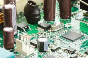
The PCB must be designed around both electrical performance and authentication requirements.
Antenna Design
The RFID antenna is one of the most important elements of the system.
Its performance depends on factors such as:
- Operating frequency
- Antenna geometry
- PCB dimensions
- Substrate properties
- Nearby metal
- Dielectric materials
- Ground-plane configuration
- Installation environment
An antenna designed for a free-space application may behave differently when embedded inside a metal enclosure, product package, or electronic assembly.
Therefore, antenna design should be validated under the actual installation conditions.
RF Matching
RFID circuits may require impedance matching between the antenna and RFID IC.
Poor matching can reduce energy transfer and communication performance, resulting in shorter read range or inconsistent identification.
For this reason, PCB fabrication tolerances and material characteristics can become important in RFID applications, particularly when the antenna is integrated directly into the PCB.
Board Geometry
The physical size and shape of the PCB can influence antenna performance.
In applications where the RFID PCB must fit inside a small product, the PCB layout may need to combine:
- RFID antenna
- Digital circuitry
- Power circuitry
- Sensors
- Identification features
This requires careful electromagnetic and mechanical design.
Materials Used for RFID PCBs
Material selection depends heavily on the RFID frequency, antenna configuration, environmental conditions, mechanical structure, and cost requirements.
FR-4
FR-4 is suitable for many conventional RFID PCB applications where standard PCB performance is sufficient.
It offers a practical combination of mechanical strength, electrical insulation, manufacturability, and cost.
High-Frequency Materials
RFID applications operating at higher frequencies may require closer attention to dielectric properties and signal behavior.
For demanding RF designs, material selection should consider dielectric constant, loss characteristics, thickness, and manufacturing consistency.
Flexible Materials
Flexible substrates can be useful when an RFID circuit needs to conform to curved surfaces or fit into compact products.
Specialized Materials
Certain applications may require materials with enhanced thermal stability, dimensional stability, or environmental resistance.
The material should always be selected according to the complete RF and mechanical design rather than based solely on the desired anti-counterfeit function.
Manufacturing Technologies for RFID PCBs
Reliable RFID PCB manufacturing requires control of both conventional PCB processes and RF-related characteristics.
Depending on the design, the manufacturing process may include:
- Material preparation
- Circuit imaging
- Etching
- Lamination
- Drilling
- Copper plating
- Surface finishing
- Solder mask
- Silkscreen or identification marking
- PCB profiling
- Electrical testing
- RFID functional verification
For more complex boards, additional processes may be required.
These can include:
- Fine-line fabrication
- Multilayer construction
- Blind or buried vias
- Microvias
- Via filling
- Edge plating
- Controlled impedance
- Special surface finishes
- Embedded or integrated structures
GOPCBA provides PCB manufacturing services covering prototype and production requirements for conventional and advanced PCB structures. PCB Manufacturing Services
Can PCB Materials Create a Unique Anti-Counterfeit Signature?
Some specialized anti-counterfeit systems can incorporate unique physical or chemical markers into materials, coatings, inks, or encapsulation structures.
However, these features should not be treated as standard characteristics of ordinary PCB materials.
If a product requires a physical unclonable feature or material-based authentication mechanism, it should be deliberately engineered into the security architecture.
Possible approaches may include:
- Specialized security inks
- Micro-marking
- Tamper-evident structures
- Unique serialized markings
- Controlled material identifiers
- Embedded security elements
- Cryptographic RFID functions
- Secure backend authentication
The important principle is that the security feature must be designed, documented, controlled, and verified.
Simply using a non-standard PCB material does not automatically create a secure anti-counterfeit system.
Traceability: Connecting the PCB to Its Manufacturing History
Manufacturing traceability can significantly strengthen an RFID PCB authentication system.
A unique PCB or RFID identifier can potentially be associated with manufacturing information such as:
- Material batch
- Production date
- Manufacturing order
- PCB revision
- Process route
- Inspection results
- RFID IC information
- Testing records
This creates a digital manufacturing history for the physical PCB.
For example:
PCB ID → Manufacturing Record → RFID ID → Product ID → Supply Chain Record
When a product is inspected, the RFID identifier can be compared with the corresponding manufacturing record.
This makes unauthorized replacement or duplication more difficult because the identifier is linked to information that exists outside the physical PCB itself.
RFID PCB Anti-Counterfeit Security Should Use Multiple Layers
A robust anti-counterfeit system should avoid relying on one authentication mechanism.
A layered architecture may combine four major elements.
Layer 1: Physical Security
Physical security features may include:
- Tamper-evident construction
- Hidden markings
- Micro-identification
- Specialized packaging
- Controlled PCB geometry
These features make unauthorized physical replication more difficult.
Layer 2: Electronic Identification
The RFID IC provides an electronic identity that can be read by a compatible system.
Depending on the RFID technology, the device may contain a unique identifier or additional memory.
Layer 3: Digital Security
More advanced systems can use cryptographic techniques to authenticate devices or verify data integrity.
This can provide stronger protection than relying solely on a static identifier.
Layer 4: Backend Traceability
The RFID identifier can be connected to a secure database containing authorized product and manufacturing records.
This enables verification throughout the supply chain.
The combination of these layers is generally much stronger than any individual security feature.
Quality Control for RFID PCB Manufacturing
RFID PCBs require normal PCB quality controls plus application-specific validation.
Dimensional Inspection
PCB dimensions, hole locations, edge features, and other mechanical characteristics should be checked against the approved design.
Electrical Testing
Electrical testing can identify opens, shorts, and other connectivity problems.
Visual Inspection
The manufacturer should inspect:
- Surface condition
- Solder mask
- Copper features
- Markings
- Board edges
- Plated holes
RF Performance Verification
For RFID-specific applications, functional testing may be required to verify:
- RFID communication
- Read/write functionality where applicable
- Antenna performance
- Frequency response
- Read range
- Matching characteristics
The exact test method should be defined according to the RFID technology and final application.
RFID PCB Manufacturing for High-Frequency Applications
RFID systems can operate across different frequency ranges, and PCB design requirements vary accordingly.
For higher-frequency applications, PCB manufacturing tolerances and material properties can have a greater influence on RF behavior.
Important factors include:
- Dielectric constant
- Dielectric thickness
- Copper thickness
- Copper surface characteristics
- Trace geometry
- Antenna dimensions
- Layer configuration
- Ground-plane design
- Manufacturing tolerances
A PCB manufacturer should therefore understand the relationship between fabrication variation and RF performance.
For demanding RF designs, GOPCBA can support high-frequency PCB manufacturing requirements where material selection and controlled fabrication are important to circuit performance. High-Frequency PCB Manufacturing
Applications of Anti-Counterfeit RFID PCBs
Anti-counterfeit RFID PCB technology can be adapted to many industries.
Pharmaceutical Products
Pharmaceutical supply chains require reliable product identification and traceability.
An RFID-based identification system can associate a product or package with a unique electronic identity, helping authorized parties verify supply-chain information.
For high-value or regulated products, additional security mechanisms may be integrated into the authentication architecture.
Luxury Goods
Luxury products are frequently targeted by counterfeiters.
Compact RFID PCB assemblies can potentially be integrated into:
- Hardware components
- Product tags
- Packaging
- Accessories
- Identification modules
The RFID identifier can then be associated with the product’s manufacturing and distribution information.
Electronic Components
Counterfeit electronic components can create serious reliability and supply-chain risks.
RFID identification can help manufacturers and distributors associate electronic components or assemblies with authorized records.
Additional authentication technologies can provide further protection where required.
Industrial Equipment
Industrial equipment often has long service lives and may pass through multiple owners, distributors, and maintenance organizations.
An RFID identification system can help maintain a digital record of:
- Equipment identity
- Manufacturing information
- Service history
- Inspection status
- Replacement components
This extends the role of RFID beyond anti-counterfeiting into asset management and lifecycle traceability.
Automotive and Transportation Electronics
Automotive and transportation systems require strong component traceability.
RFID-enabled electronic identification can help connect components with manufacturing and quality records, particularly in supply chains where large numbers of similar components must be distinguished.
Anti-Counterfeit RFID PCB vs. Conventional RFID Tags
An RFID PCB is not necessarily better than every conventional RFID tag.
The appropriate technology depends on the application.
| Feature | Conventional RFID Tag | RFID PCB |
|---|---|---|
| Construction | Usually flexible or printed | Rigid or specialized PCB |
| Mechanical durability | Application-dependent | Generally robust |
| Circuit integration | Limited | High |
| Antenna integration | Printed/attached | Can be integrated into PCB |
| Additional electronics | Limited | Easier to integrate |
| Custom geometry | Moderate | High |
| Environmental protection | Depends on encapsulation | Can be designed for rugged environments |
| Product integration | Labels and packaging | Electronics, modules, equipment |
| Traceability | Supported | Supported |
| Anti-counterfeit capability | Depends on security architecture | Depends on security architecture |
The choice should be based on the product’s mechanical environment, RF requirements, available space, required electronics, security level, and production economics.
How to Design a Secure RFID PCB System
When developing an anti-counterfeit RFID PCB, engineers should consider the entire system rather than focusing only on the PCB.
A practical development process can include:
Step 1: Define the Security Objective
Determine what the system needs to prevent.
For example:
- Unauthorized duplication
- Product substitution
- Component replacement
- Identity cloning
- Supply-chain diversion
- Tampering
Step 2: Select the RFID Technology
Choose the appropriate RFID technology based on:
- Frequency
- Read distance
- Data requirements
- Reader infrastructure
- Environmental conditions
- Cost
Step 3: Design the PCB and Antenna
Optimize the board layout and antenna for the actual installation environment.
Step 4: Establish the Identity Architecture
Define how RFID identifiers are generated, assigned, stored, and verified.
Step 5: Connect Manufacturing Data
Link PCB and RFID identifiers with manufacturing records and product information.
Step 6: Validate the Complete System
Test the RFID PCB under realistic mechanical, electrical, environmental, and RF conditions.
This system-level approach provides a more reliable security architecture than simply adding an RFID chip to an existing PCB.
The Role of PCB Manufacturing Quality in RFID Authentication
Authentication depends on the reliability of the physical device.
If an RFID PCB suffers from manufacturing defects, antenna performance may become unstable, electrical connections may fail, or the identification system may become unreliable.
Consistent PCB fabrication is therefore important for:
- Antenna geometry
- Layer registration
- Copper thickness
- Dielectric structure
- Mechanical dimensions
- Electrical connectivity
- Long-term reliability
For advanced designs, the manufacturing process should be aligned with the electrical requirements established during PCB design.
GOPCBA also provides PCB prototype assembly capabilities, allowing engineering teams to validate RFID PCB designs through physical prototypes before moving into production. Prototype PCB Assembly
From RFID PCB Prototype to Mass Production
Prototype validation is particularly important for RFID applications because RF behavior can change when the PCB is installed into the final product.
Prototype testing should evaluate the complete system under representative conditions.
After successful validation, the design can move through:
RFID PCB Prototype → Functional Validation → Security Validation → Pilot Production → Mass Production
During production, maintaining consistent materials, PCB geometry, antenna characteristics, and RFID component specifications is important for repeatable performance.
A manufacturing partner capable of supporting both prototypes and production can help minimize differences between development samples and production boards.
For larger projects, GOPCBA’s turnkey PCB assembly capabilities can integrate PCB fabrication, component procurement, assembly, inspection, and related manufacturing processes. Turnkey PCB Assembly Services
Choosing an RFID PCB Manufacturer
When selecting an RFID PCB manufacturer, consider more than basic PCB fabrication cost.
Important evaluation criteria include:
RF and PCB Engineering Experience
The supplier should understand PCB fabrication requirements that can affect antenna and RF performance.
Manufacturing Capability
The manufacturer should support the required layer count, materials, PCB geometry, surface finish, and special processes.
Quality Control
Inspection and testing should cover both PCB manufacturing quality and application-specific requirements.
Traceability
Production records should be sufficiently controlled to support product-level traceability where required.
Prototype Support
The manufacturer should be able to produce engineering samples efficiently for design validation.
Production Scalability
A supplier should be capable of supporting the transition from prototype quantities to stable production.
Engineering Communication
Fast and accurate communication is particularly important when PCB manufacturing parameters interact with RF performance.
Why Choose GOPCBA for RFID PCB Manufacturing?
RFID PCB projects often require a combination of conventional PCB manufacturing, RF considerations, prototype validation, and production scalability.
GOPCBA supports PCB development and manufacturing across different board technologies and application requirements, helping customers move from engineering design to physical prototypes and production.
The manufacturing process can be adapted to requirements involving multilayer structures, high-frequency materials, controlled electrical characteristics, and specialized PCB constructions.
For customers developing RFID-based authentication systems, the objective is to provide a PCB platform that can be consistently manufactured and validated as part of the complete RFID system.
Conclusion
An anti-counterfeit RFID PCB can provide an effective physical foundation for product identification, authentication, and traceability when it is integrated into a properly designed security architecture.
Its effectiveness does not come from the PCB alone. Instead, reliable anti-counterfeiting depends on the interaction between:
PCB Design + RFID Technology + Secure Identification + Manufacturing Traceability + Backend Authentication
The PCB provides the physical platform for the RFID circuitry and antenna, while electronic identification and digital systems establish the product’s identity.
For demanding applications, additional security layers such as cryptographic authentication, tamper detection, controlled manufacturing data, and specialized physical markers can further strengthen the system.
As supply chains become more complex and counterfeit risks continue to affect high-value products, RFID-enabled PCB technology provides manufacturers with a flexible way to connect physical products with secure digital identities.