Photonic Integrated Circuit Hybrid PCB: Design and Manufacturing Guide
What Is a Photonic Integrated Circuit Hybrid PCB?
A Photonic Integrated Circuit Hybrid PCB is an advanced printed circuit board technology designed to support the integration of photonic devices and electronic circuits within the same system architecture. Unlike conventional PCBs, which primarily manage electrical signal transmission, hybrid photonic-electronic boards must address the requirements of both optical and electrical interconnections.
This technology is becoming increasingly important in high-performance applications such as optical communications, advanced sensing, data centers, high-speed computing, and emerging quantum technologies.
The PCB may need to provide controlled electrical impedance, low-loss signal transmission, precise mechanical positioning, thermal management, and high-density interconnection while supporting optical components such as photonic integrated circuits, optical transceivers, lasers, detectors, and coupling structures.
As optical and electronic systems continue to converge, PCB design and manufacturing accuracy become increasingly important to overall system performance.
For complex applications, an integrated approach to PCB Design and Layout can help address signal integrity, component placement, thermal requirements, and manufacturability at the early design stage.
Why Hybrid PCBs Are Important for Photonic Integration
Photonic systems can transmit large amounts of information with very low transmission loss over suitable optical paths. However, optical devices still require electronic circuits for power management, control, signal processing, monitoring, and communication with other system components.
A hybrid PCB provides the physical platform that connects these different functional domains.
Typical functions include:
- Electrical connection between control circuits and photonic devices
- High-speed data transmission
- Power distribution
- Optical component positioning
- Thermal management
- High-density component integration
- Signal conditioning and monitoring
- Mechanical support for optical and electronic assemblies
The challenge is that optical and electrical systems have different performance requirements. Electrical signals are sensitive to impedance discontinuities, dielectric properties, crosstalk, and electromagnetic interference, while optical systems can be sensitive to alignment accuracy, coupling efficiency, vibration, and thermal variation.
Therefore, the PCB must be designed as part of the complete electro-optical system rather than as an isolated electronic component.
Key Technical Characteristics of Photonic Integrated Circuit Hybrid PCB
Low-Loss Electrical Signal Transmission
High-speed optical systems still contain high-speed electrical interfaces between components such as processors, drivers, receivers, transimpedance amplifiers, and photonic integrated circuits.
The PCB dielectric material, copper surface characteristics, trace geometry, and layer structure can all affect electrical insertion loss.
For high-frequency interfaces, selecting appropriate materials and maintaining controlled impedance are essential for minimizing signal degradation.
This makes High-Frequency PCB technology particularly relevant to optical communication and photonic-electronic systems.
Controlled Impedance
High-speed electrical interfaces commonly require tightly controlled impedance.
Impedance is influenced by:
- Trace width
- Copper thickness
- Dielectric thickness
- Dielectric constant
- Reference-plane configuration
- Surface roughness
- Via structures
A change in any of these parameters can affect signal integrity.
For differential interfaces, maintaining consistent geometry between paired traces is also important. Unequal routing, excessive via transitions, or poorly designed reference-plane transitions may increase reflection and differential skew.
High-Density Interconnection
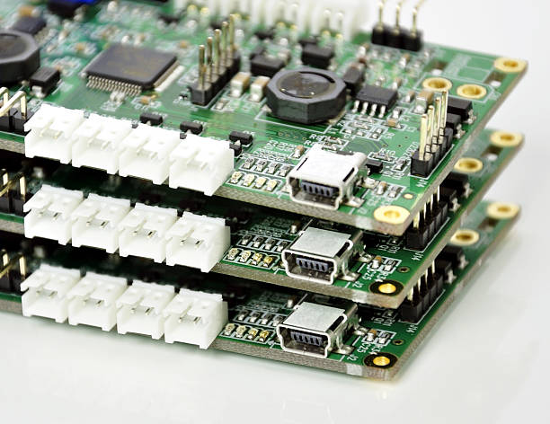
Photonic integrated systems often require compact packaging because optical components and electronic control circuits must be located close to each other.
This creates demand for:
- Fine-line circuitry
- Microvias
- Blind and buried vias
- High-density multilayer structures
- Fine-pitch component footprints
- Advanced surface finishes
- Precise layer registration
Microvia technology can help designers create compact interconnection structures while reducing routing congestion.
However, smaller geometries also increase manufacturing sensitivity, making process control essential.
Materials Used in Photonic Hybrid PCB Construction
Material selection is one of the most important considerations in photonic-electronic PCB design.
Different areas of a hybrid PCB may have different electrical, thermal, mechanical, and optical requirements.
High-Frequency Materials
High-frequency laminate materials can be used where high-speed electrical signals require lower dielectric loss and more stable electrical characteristics.
Important parameters may include:
- Dielectric constant
- Dissipation factor
- Thermal stability
- Dimensional stability
- Copper adhesion
- Moisture resistance
Material selection should be based on the actual operating frequency, signal speed, environmental conditions, and manufacturing structure.
Hybrid Dielectric Construction
Some applications may require multiple materials within the same PCB stackup.
For example, a hybrid construction can combine conventional structural materials with higher-performance materials in selected signal layers.
This approach can balance:
- Electrical performance
- Mechanical stability
- Thermal performance
- Manufacturing cost
- Overall board thickness
However, different materials can have different coefficients of thermal expansion and lamination characteristics. The stackup therefore needs to be engineered carefully to minimize dimensional and reliability problems.
Thermally Stable Materials
Photonic components can be sensitive to temperature because optical characteristics may change with thermal conditions.
PCB materials with suitable thermal stability can help maintain mechanical and electrical consistency during operation.
Thermal management should nevertheless be considered at the complete assembly level rather than relying on the PCB material alone.
Manufacturing Challenges of Photonic Integrated Circuit Hybrid PCB
The manufacturing process for a Photonic Integrated Circuit Hybrid PCB can be significantly more demanding than conventional PCB production.
Several manufacturing variables must be controlled simultaneously.
Material Compatibility
Different laminate systems can have different:
- Thermal expansion coefficients
- Resin content
- Glass-transition temperatures
- Lamination pressures
- Curing characteristics
- Moisture absorption behavior
When different materials are combined in one multilayer structure, manufacturing engineers must establish an appropriate lamination process.
Poor material compatibility can result in:
- Board warpage
- Delamination
- Dimensional instability
- Registration errors
- Reliability problems
Precision Drilling and Microvias
High-density photonic-electronic assemblies may require very small interconnection structures.
Laser drilling can be used to create microvias for high-density routing.
The manufacturing process must control:
- Hole diameter
- Hole depth
- Position accuracy
- Copper coverage
- Via filling
- Registration
When microvias are stacked or combined with other via structures, process control becomes even more important.
Resin-Filled Vias
Resin-filled vias can provide a planar surface and support high-density component placement.
Proper filling is important because voids or incomplete filling can affect:
- Mechanical reliability
- Surface flatness
- Subsequent copper plating
- Component placement
- Electrical performance
The appropriate via structure should therefore be selected during PCB design rather than added late in manufacturing.
Layer Registration and Dimensional Accuracy
Photonic systems often require precise positioning of optical and electronic components.
Layer-to-layer registration is therefore an important manufacturing parameter.
Registration errors can affect:
- Fine-pitch pads
- Microvia connections
- Differential routing
- Controlled-impedance structures
- Optical component interfaces
- Mechanical alignment features
Thermal expansion during lamination can cause dimensional changes. PCB manufacturers must therefore account for material behavior and process variation when developing fabrication parameters.
For demanding designs, PCB Manufacturing should be evaluated together with the PCB stackup and fabrication tolerances before production begins.
Surface Finish Considerations
Surface finish selection can affect solderability, contact reliability, wire bonding compatibility, and long-term stability.
Potential surface finishes include:
- ENIG
- ENEPIG
- HASL
- Immersion silver
- OSP
The appropriate finish depends on the application and assembly process.
For advanced photonic-electronic assemblies, ENIG or ENEPIG may be considered where fine-pitch components, wire bonding, or specific contact requirements are involved.
The final selection should be based on component requirements, assembly technology, environmental conditions, and expected service life.
Thermal Management in Photonic Hybrid PCBs
Thermal management is particularly important when a PCB integrates high-speed electronic devices with photonic components.
Heat-generating devices may include:
- Laser drivers
- Optical transceivers
- High-speed processors
- Power management ICs
- RF circuits
- Amplifiers
Excessive temperature can affect electronic reliability and may also influence optical characteristics.
Thermal Vias
Thermal vias can transfer heat from component pads or thermal areas into internal copper planes.
A suitable thermal-via structure can improve heat spreading while also supporting electrical grounding where appropriate.
Copper Planes
Large copper planes can distribute heat across the PCB.
They can also provide low-impedance power and ground paths, making them useful for both thermal and electrical design.
Component Placement
Thermal design should begin with component placement.
High-power components should be positioned so that heat can be efficiently transferred toward heat sinks, chassis structures, or other thermal paths.
Signal Integrity and EMI Control
A photonic system may contain multiple high-speed electrical interfaces operating close to sensitive analog, optical-control, or power circuits.
Poor PCB layout can introduce:
- Crosstalk
- Ground bounce
- Electromagnetic interference
- Signal reflection
- Common-mode noise
- Power integrity problems
Effective layout techniques include:
- Maintaining continuous reference planes
- Minimizing unnecessary trace transitions
- Keeping differential pairs properly coupled
- Controlling impedance
- Separating sensitive analog and noisy digital circuits
- Minimizing high-current loop areas
- Using appropriate filtering and shielding
High-speed traces should also be routed with careful attention to via transitions and return-current paths.
PCB Assembly for Photonic Integrated Systems
Manufacturing the bare board is only one part of the production process.
The assembly stage determines whether the PCB can reliably support the required photonic and electronic components.
A typical PCB Assembly process may include:
- Solder paste printing
- Component placement
- Reflow soldering
- Through-hole assembly where required
- Inspection
- Electrical testing
- Functional testing
Advanced photonic assemblies may also require special processes for fine-pitch devices, optical components, connectors, or wire-bonded components.
Fine-Pitch Component Assembly
High-density photonic systems can contain small packages and closely spaced pads.
Accurate solder paste deposition and component placement are important to reduce:
- Solder bridges
- Insufficient solder
- Component misalignment
- Open joints
- Tombstoning
Automated optical inspection can help identify many visible assembly defects.
X-Ray Inspection
X-ray inspection can be useful for packages and solder joints that cannot be fully inspected optically.
It can help identify:
- Voids
- Hidden solder defects
- Internal connection problems
- BGA soldering issues
The inspection strategy should be matched to the component technology and reliability requirements.
Quality Control for Photonic Hybrid PCB Manufacturing
Because photonic-electronic systems can be highly sensitive to small manufacturing variations, quality control should cover the entire production process.
Incoming Material Inspection
Materials should be checked against the approved specifications.
Important parameters may include:
- Material type
- Thickness
- Copper thickness
- Dielectric characteristics
- Surface condition
- Dimensional stability
In-Process Inspection
Manufacturing inspection can monitor:
- Trace geometry
- Registration
- Hole dimensions
- Plating quality
- Via structures
- Surface finish
- Lamination quality
Electrical Testing
Electrical testing can identify problems such as:
- Opens
- Shorts
- Isolation failures
- Connection defects
For high-speed boards, additional signal-integrity verification may be required depending on the design.
Prototype Development and Design Validation
Photonic hybrid PCB projects should ideally be validated through prototypes before entering higher-volume production.
Prototype evaluation can reveal issues involving:
- Signal integrity
- Thermal performance
- Optical alignment
- Component compatibility
- Mechanical interfaces
- Assembly yield
- Manufacturing tolerances
Using Prototype PCB Assembly can help engineering teams evaluate the complete electronic assembly before committing to larger production volumes.
Prototype testing can also provide useful feedback for optimizing the PCB stackup, component placement, routing, thermal structure, and manufacturing process.
Applications of Photonic Integrated Circuit Hybrid PCB
Optical Communication
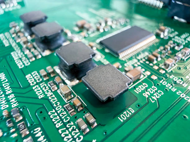
One of the most important applications is optical communication.
Photonic-electronic PCBs can support:
- Optical transceiver modules
- Data center interconnects
- High-speed communication equipment
- Optical networking systems
- Advanced telecommunications infrastructure
The combination of optical transmission and high-speed electronic control can support higher bandwidth and more efficient data transmission architectures.
Advanced Sensing
Photonic systems are also used in sensing technologies.
Potential applications include:
- Optical sensors
- Industrial measurement
- Environmental monitoring
- Imaging systems
- Precision instrumentation
The PCB provides the electrical interface and control architecture required by the optical sensing system.
High-Performance Computing
As computing systems require increasing data bandwidth, optical interconnect technologies are becoming increasingly relevant.
Photonic-electronic integration can support high-bandwidth connections between computing, memory, networking, and acceleration systems.
Quantum Technologies
Photonic technologies are also being explored in quantum computing, quantum communication, and quantum sensing.
These applications can impose particularly demanding requirements for signal integrity, thermal stability, electromagnetic noise control, and mechanical precision.
Components and Supply Chain Considerations
Photonic hybrid PCB projects can involve specialized components and materials that are not always interchangeable.
The bill of materials may include:
- Photonic integrated circuits
- Optical transceivers
- Laser drivers
- Photodetectors
- High-speed processors
- RF components
- Connectors
- Precision passive components
- Specialized PCB materials
Early component planning is therefore important.
A comprehensive Components Procurement strategy can help engineering teams evaluate component availability, approved alternatives, lifecycle considerations, and supply-chain risks before production.
Designing Photonic Hybrid PCBs for Manufacturability
Design for manufacturability should be considered from the beginning of the project.
Important DFM considerations include:
- PCB material availability
- Stackup complexity
- Minimum trace and spacing
- Via dimensions
- Microvia structures
- Copper thickness
- Lamination sequence
- Surface finish
- Component package selection
- Assembly clearances
- Testing requirements
A technically possible PCB design is not necessarily an economically or consistently manufacturable design.
Early collaboration between PCB designers, manufacturers, and assembly engineers can identify potential production problems before fabrication begins.
Future Development of Photonic Integrated Circuit Hybrid PCBs
The continued growth of data-intensive applications is likely to increase demand for tighter optical-electronic integration.
Future development may focus on:
- Higher-density interconnection
- More compact optical modules
- Lower-loss electrical interfaces
- Advanced multilayer structures
- Improved thermal management
- Greater automation
- More precise optical alignment
- Advanced packaging technologies
The boundary between PCB technology, semiconductor packaging, optical packaging, and photonic integration is becoming increasingly interconnected.
As a result, PCB manufacturers supporting photonic applications will need to manage not only conventional PCB fabrication but also increasingly complex material, dimensional, electrical, and assembly requirements.
Why Photonic Integrated Circuit Hybrid PCB Quality Matters
A Photonic Integrated Circuit Hybrid PCB is more than a conventional circuit board with optical components attached.
It is an enabling platform for integrating optical transmission, electronic processing, power delivery, thermal management, and mechanical structures within a compact system.
Successful implementation requires careful attention to material selection, controlled impedance, signal integrity, layer registration, microvia technology, thermal management, surface finish, assembly accuracy, and quality inspection.
For engineers developing optical communication, sensing, computing, or other advanced photonic systems, selecting an appropriate PCB manufacturing and assembly process early in the project can significantly reduce design and production risks.
Conclusion
Photonic Integrated Circuit Hybrid PCB technology plays an important role in the continued convergence of photonics and electronics. By combining high-speed electrical interconnection with structures capable of supporting photonic components, hybrid PCBs provide a practical foundation for advanced optical and electronic systems.
The most demanding applications require more than conventional PCB fabrication. Material compatibility, low-loss signal transmission, controlled impedance, high-density interconnection, precision registration, thermal management, and advanced assembly processes must all be considered as part of a complete engineering strategy.
As optical communication, high-performance computing, sensing, and emerging photonic technologies continue to develop, reliable hybrid PCB design and manufacturing will remain an important factor in achieving system-level performance and scalability.