What Is a High-Speed Rail Signaling PCB?
A High-Speed Rail Signaling PCB is a printed circuit board designed for electronic systems used in railway signaling, train control, communication, monitoring, and other safety-critical railway applications.
Railway signaling equipment operates under demanding environmental and electrical conditions. Compared with many consumer electronics applications, these systems may need to withstand temperature variation, vibration, electromagnetic interference, humidity, and long operating cycles.
The PCB serves as the electrical and mechanical foundation for components such as processors, communication interfaces, power circuits, signal-conditioning circuits, sensors, and control modules.
For this reason, a Railway Signaling PCB must be designed around reliability rather than simply cost or component density.
The complete development process typically involves:
- Material selection
- Multilayer stackup design
- Signal integrity analysis
- Power integrity optimization
- Thermal management
- EMC/EMI control
- Precision fabrication
- PCB assembly
- Electrical and environmental testing
A reliable railway PCB manufacturing strategy begins at the design stage. Professional PCB Design and Layout can help engineers evaluate stackup construction, impedance requirements, routing, grounding, thermal management, and manufacturability before production.
Why Railway Signaling PCBs Require High Reliability
Railway signaling systems are responsible for processing and transmitting information related to train operation and infrastructure status. A failure in electronic hardware can potentially affect system availability and maintenance requirements.
Therefore, railway electronics are generally designed with greater emphasis on:
- Long-term stability
- Electrical reliability
- Mechanical robustness
- EMC performance
- Environmental resistance
- Traceability
- Consistent manufacturing quality
A High-Reliability PCB must maintain its electrical and mechanical characteristics throughout its expected service environment.
This requires coordination between PCB design, materials, fabrication, assembly, and system-level validation.
Environmental Requirements for High-Speed Rail Signaling PCB
One of the most important challenges in railway PCB development is environmental reliability.
Temperature Cycling
Railway equipment can be exposed to significant temperature changes depending on installation location, climate, enclosure design, and operating conditions.
Temperature cycling can create mechanical stress because different materials expand and contract at different rates.
Repeated thermal cycling may contribute to:
- Delamination
- Copper fatigue
- Plated-hole stress
- Solder-joint fatigue
- Dimensional changes
A suitable laminate system, controlled lamination process, and appropriate PCB structure can help reduce these risks.
Instead of applying one universal temperature range to every railway PCB, engineers should define the required environmental conditions according to the equipment location and applicable railway specifications.
Vibration and Mechanical Shock
Railway equipment is continuously exposed to mechanical vibration.
The PCB and components must therefore be designed to withstand the expected mechanical loads.
Important considerations include:
- Board thickness
- PCB mounting points
- Component weight
- Connector design
- Hole structure
- Copper distribution
- Solder-joint reliability
- Mechanical reinforcement
Mechanical design and PCB layout should be evaluated together.
Heavy components should be positioned carefully, and mounting holes should provide sufficient mechanical support without compromising electrical routing.
Electromagnetic Compatibility in Railway Signaling PCB Design
Electromagnetic compatibility is another critical consideration.
Railway environments can contain electrical equipment capable of generating electromagnetic noise. Motors, power conversion equipment, switching circuits, communication systems, and high-voltage infrastructure can all contribute to a challenging electromagnetic environment.
A Railway Signaling PCB therefore needs an appropriate EMC strategy.
Important techniques include:
- Ground-plane optimization
- Controlled return paths
- Differential signaling
- Signal-layer planning
- Power-plane separation
- Shielding
- Filtering
- Proper connector design
- Controlled impedance
EMC should not be treated as a final-stage problem.
The PCB stackup and routing architecture should be developed with signal integrity and electromagnetic compatibility in mind from the beginning.
Controlled Impedance for Railway Signaling PCB
Modern railway signaling equipment can include high-speed digital interfaces and communication circuits.
When signals travel through high-speed transmission lines, impedance discontinuities can cause:
- Reflections
- Signal distortion
- Crosstalk
- Timing problems
- Increased electromagnetic emissions
The characteristic impedance of a PCB transmission line depends on factors such as:
- Trace width
- Trace thickness
- Dielectric thickness
- Dielectric constant
- Reference-plane configuration
- Copper surface characteristics
For differential pairs, trace spacing and symmetry are also important.
An impedance requirement should therefore be defined according to the actual circuit design and interface specifications.
Rather than assuming a single tolerance applies to every application, the PCB manufacturer should work from the customer’s specified impedance target and verify the finished board using appropriate testing methods.
High-Speed PCB Materials for Railway Electronics
Material selection has a direct influence on electrical and mechanical performance.
Standard FR-4 materials can be suitable for many railway electronic circuits, but specialized materials may be considered when the design requires improved thermal stability, lower dielectric loss, controlled dielectric properties, or other specific characteristics.
Potential material considerations include:
High-Tg Materials
High-Tg laminates can provide improved thermal stability compared with conventional materials and may be considered for applications involving elevated operating temperatures or demanding thermal cycles.
Low-Loss Materials
High-speed communication circuits may require materials with lower dielectric loss and more stable electrical characteristics.
These materials can be useful where signal integrity is a major design consideration.
Low-CTE Materials
Materials with controlled coefficients of thermal expansion can help manage dimensional stability and reduce thermal-mechanical stress in demanding multilayer constructions.
The best material should always be selected according to the electrical, mechanical, thermal, and environmental requirements of the actual railway system.
Multilayer PCB Construction for Railway Signaling Systems
Railway control electronics can require multiple functional circuits within a limited enclosure.
A multilayer PCB allows engineers to integrate:
- Signal layers
- Ground planes
- Power planes
- High-speed routing
- Low-speed control circuits
- Communication interfaces
A well-designed stackup can improve signal integrity while reducing EMI and simplifying routing.
For example, high-speed signal layers can be placed adjacent to continuous reference planes to create controlled return paths.
Power and ground structures can also be planned to reduce unwanted voltage fluctuations and noise coupling.
When multilayer complexity increases, fabrication capability becomes increasingly important. Registration accuracy, lamination consistency, via reliability, and dielectric thickness control can all affect final electrical performance.
Precision Drilling and Microvia Technology
Advanced railway electronics may use compact components and high-density interconnections.
Microvias and other advanced via structures can help designers reduce PCB size and improve routing density.
Precision drilling processes must control:
- Hole diameter
- Hole position
- Hole depth
- Aspect ratio
- Layer registration
- Plating quality
- Via-to-pad alignment
For HDI structures, laser drilling may be used where appropriate.
The manufacturing process must ensure that vias provide stable electrical connections throughout the expected operating life.
PCB Surface Finish for Railway Electronics
Surface finish influences solderability, contact reliability, corrosion resistance, and long-term assembly performance.
Common PCB surface finishes include:
- ENIG
- ENEPIG
- HASL
- Lead-free HASL
- OSP
- Immersion silver
- Hard gold
The appropriate finish depends on the component package, assembly process, contact requirements, environmental conditions, and expected service life.
For fine-pitch components, a relatively flat surface finish may be beneficial for consistent solder paste deposition and component placement.
For connector contacts or wear-prone surfaces, a suitable gold finish may be considered where required by the mechanical interface.
PCB Manufacturing Process for Railway Signaling Applications
The PCB Manufacturing process must be tightly controlled when producing boards for demanding railway electronics.
A typical manufacturing workflow includes:
- Engineering review
- Material verification
- Inner-layer imaging
- Etching
- Lamination
- Mechanical or laser drilling
- Desmear and metallization
- Copper plating
- Outer-layer imaging
- Solder mask application
- Surface finishing
- Electrical testing
- Final inspection
Each stage can influence the reliability of the finished PCB.
For example, inadequate lamination control can contribute to internal defects, while drilling and plating variations can affect plated-through-hole reliability.
A structured PCB Manufacturing process should therefore integrate engineering review, process control, inspection, and testing rather than treating PCB fabrication as a simple production step.
Quality Control for High-Reliability PCB Production
Quality control is particularly important for a High-Reliability PCB.
The inspection strategy should cover both incoming materials and finished products.
Incoming Material Inspection
Materials should be verified against approved specifications.
Inspection may include:
- Laminate type
- Board thickness
- Copper thickness
- Material lot information
- Surface condition
- Dimensional characteristics
Correct material identification is essential when multiple laminate types are used.
Automated Optical Inspection
AOI can detect many defects in PCB circuitry, including:
- Open traces
- Short circuits
- Pattern abnormalities
- Missing features
- Excess or insufficient copper patterns
AOI is particularly useful for multilayer and fine-line PCB production.
X-Ray Inspection
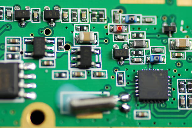
X-ray inspection can provide additional visibility into internal structures that cannot be evaluated through conventional optical inspection.
Depending on the PCB structure, it may help evaluate:
- Hidden solder joints
- Via structures
- Internal connections
- Certain assembly defects
Electrical Testing
Electrical testing can identify opens, shorts, insulation problems, and other connectivity defects.
For controlled-impedance designs, impedance testing can also verify whether critical transmission-line structures meet the specified electrical requirements.
Reliability Testing for Railway Signaling PCB
Testing requirements should be based on the actual application, system architecture, and applicable railway standards.
Potential validation categories include:
Thermal Testing
Thermal testing evaluates PCB behavior under specified temperature conditions and thermal cycling.
It can help identify problems associated with:
- Material expansion
- Delamination
- Copper fatigue
- Solder-joint degradation
Humidity Testing
Moisture can influence insulation resistance, corrosion, and material stability.
Humidity testing can therefore be useful for equipment expected to operate in humid or variable environments.
Vibration Testing
Mechanical vibration testing evaluates the structural integrity of the assembled PCB.
It can help identify weaknesses in:
- Solder joints
- Connectors
- Heavy components
- PCB mounting structures
- Mechanical interfaces
Electrical Testing
Electrical validation confirms that circuits maintain the required electrical characteristics.
Testing may include:
- Continuity
- Isolation
- Insulation resistance
- Dielectric withstand
- Functional testing
- Impedance verification
The exact test program should be determined by the product specification and applicable standards.
PCB Assembly for Railway Signaling Equipment
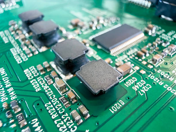
Bare-board quality alone cannot guarantee the reliability of a railway electronic system.
The component assembly process is equally important.
A professional PCB Assembly process may include:
- Solder paste printing
- SMT placement
- Reflow soldering
- Through-hole assembly
- AOI
- X-ray inspection
- Electrical testing
- Functional testing
Component selection and PCB assembly parameters should be considered together.
Components used in railway electronics may need to satisfy specific temperature, reliability, lifecycle, or environmental requirements.
Solder-joint quality is also important because continuous vibration and thermal cycling can place mechanical stress on assembled components.
Design for Manufacturability of Railway Signaling PCB
Design for manufacturability should be incorporated before PCB production begins.
Important DFM considerations include:
- Minimum trace width and spacing
- Via size
- Hole-to-copper clearance
- Board thickness
- Copper thickness
- Layer count
- Impedance requirements
- Component spacing
- Assembly clearances
- Panelization
- Test-point placement
- Mechanical mounting features
A DFM review can identify problems before they reach production.
For example, a design may meet electrical requirements but contain insufficient clearance for a manufacturing process or create unnecessary assembly complexity.
Early engineering communication can reduce redesigns and improve production consistency.
Prototype Validation for Railway PCB Projects
Prototype production is an important step when developing new railway electronic equipment.
A prototype can be used to validate:
- PCB stackup
- Material selection
- Signal integrity
- Impedance
- Thermal behavior
- Mechanical fit
- Component compatibility
- Assembly performance
- Functional operation
For early-stage projects, Prototype PCB Assembly allows engineers to evaluate both the bare PCB and assembled electronics before moving to larger production quantities.
Prototype testing can reveal issues that may not be visible in simulation or schematic review.
This is especially valuable for complex multilayer boards, high-speed communication circuits, and mechanically constrained railway equipment.
Traceability in Railway PCB Manufacturing
Traceability is an important part of high-reliability electronic manufacturing.
A robust traceability system can associate production information with specific PCB batches or manufacturing lots.
Potential records include:
- Material lot
- Production date
- Process parameters
- Inspection results
- Electrical test results
- Surface finish information
- Assembly records
- Component lot information
Traceability makes it easier to investigate manufacturing issues and support corrective actions.
For long-life products, maintaining reliable production records can also help with future replacement, maintenance, and engineering changes.
Component Supply Chain Management
Railway electronics can have long product lifecycles, making component availability an important engineering consideration.
A PCB project should consider:
- Component lifecycle
- Approved alternatives
- Lead times
- Obsolescence risks
- Supplier qualification
- Lot traceability
- Long-term availability
Component selection should ideally be performed together with PCB design rather than after the board has already been finalized.
For projects requiring integrated procurement and assembly, Components Procurement can help coordinate component sourcing with PCB fabrication and production planning.
How to Select a High-Speed Rail Signaling PCB Manufacturer
Choosing a suitable PCB supplier requires more than comparing unit prices.
Important evaluation criteria include:
Engineering Capability
The supplier should understand multilayer PCB construction, signal integrity, impedance control, thermal management, and manufacturability.
Material Capability
The manufacturer should have experience with the laminate systems required by the project.
Manufacturing Capability
Relevant capabilities may include:
- Multilayer PCB fabrication
- HDI
- Controlled impedance
- High-density routing
- Advanced drilling
- Special surface finishes
- Precision registration
- High-reliability fabrication
Quality Management
The supplier should maintain documented inspection and testing procedures appropriate to the application.
Assembly Capability
Integrated PCB fabrication and assembly can simplify supplier communication and reduce coordination between multiple manufacturing partners.
Traceability
A clear traceability system can support quality investigations and long-term product management.
Railway PCB Manufacturing and Industry Standards
Railway electronic equipment may be subject to application-specific standards and customer requirements.
Depending on the product and market, relevant requirements can address areas such as:
- Electronic equipment reliability
- Environmental conditions
- Electromagnetic compatibility
- Fire and smoke performance
- Software and system safety
- Manufacturing quality
The exact compliance requirements depend on the equipment type, installation environment, railway system, and target market.
PCB manufacturers should therefore work from the customer’s approved specifications and applicable standards instead of assuming that one certification or testing program covers every railway PCB application.
Future Trends in Railway Signaling PCB Technology
Railway signaling systems are becoming increasingly digital and interconnected.
Future PCB requirements are likely to be influenced by:
- Higher-speed communication
- More compact electronic systems
- Increased computing requirements
- Advanced train control
- Condition monitoring
- Predictive maintenance
- Industrial networking
- Increased system integration
These developments will increase demand for PCBs capable of combining high-speed digital circuits, RF communication, power management, and control electronics within compact form factors.
As signal speeds increase, impedance control, low-loss materials, grounding, thermal management, and EMC engineering will become increasingly important.
At the same time, long product lifecycles will continue to make reliability, traceability, and component availability major considerations.
Why High-Speed Rail Signaling PCB Quality Matters
The PCB is a fundamental hardware element of modern railway electronic systems.
A reliable High-Speed Rail Signaling PCB requires coordinated engineering across:
- Material selection
- PCB layout
- Stackup design
- Signal integrity
- EMC control
- Thermal management
- Precision fabrication
- PCB assembly
- Electrical testing
- Environmental validation
- Traceability
High-quality manufacturing is not simply about producing a board that passes an electrical continuity test. The goal is to create a PCB that consistently maintains its required electrical, mechanical, and environmental performance throughout its intended service life.
For railway signaling applications, this reliability-oriented approach can reduce field failures, maintenance risks, and production inconsistencies.
Conclusion
High-Speed Rail Signaling PCB technology plays an important role in modern railway control, communication, monitoring, and signaling equipment.
Because these systems operate in demanding environments, PCB design and manufacturing must address temperature variation, vibration, electromagnetic interference, signal integrity, mechanical strength, and long-term reliability.
The most effective approach is to integrate PCB design, material selection, manufacturing engineering, assembly, testing, and traceability into one controlled development process.
From multilayer and high-speed PCB structures to precision drilling, controlled impedance, specialized materials, and advanced inspection, every stage can influence final system performance.
By working with an experienced PCB manufacturing and assembly partner, railway electronics developers can better manage manufacturing risks and build reliable electronic hardware for demanding transportation applications.
As railway systems become more connected, intelligent, and data-driven, the requirements for high-reliability PCB technology will continue to evolve. Advanced Railway Signaling PCB solutions will remain an essential foundation for the next generation of safe, efficient, and connected rail transportation systems.
:::