Special Material PCB Manufacturing Services: Materials, Processes and Quality Control
What Is a Special Material PCB?
A Special Material PCB is a printed circuit board manufactured using advanced or application-specific materials that provide electrical, thermal, mechanical, or environmental properties beyond those typically offered by standard FR-4.
These PCBs are increasingly used in demanding electronic systems, including:
- Industrial automation
- Medical electronics
- Automotive electronics
- High-frequency communications
- Power electronics
- Flexible electronics
- Aerospace and other high-reliability applications
Unlike conventional FR-4 circuit boards, special material PCBs may require more complex fabrication processes because different materials behave differently during drilling, etching, lamination, plating, and thermal processing.
The material itself can directly influence signal loss, impedance stability, thermal performance, dimensional stability, flexibility, and long-term reliability.
For this reason, successful Special Material PCB Manufacturing requires more than simply selecting an advanced laminate. Material properties must be considered together with stackup design, fabrication parameters, assembly requirements, and the intended operating environment.
For complex projects, professional PCB Design and Layout can help engineers evaluate material selection, stackup construction, controlled impedance, thermal requirements, and manufacturability before production begins.
Why Special Material PCB Manufacturing Requires Specialized Processes
The main challenge of Special Material PCB Manufacturing is the wide variation in material characteristics.
Different applications may require completely different material systems.
For example, high-frequency communication equipment may require PTFE-based or other low-loss laminates, while high-current applications may use heavy copper constructions. Flexible and rigid-flexible applications require materials capable of repeated bending and appropriate dimensional stability.
Common special PCB material categories include:
- High-frequency laminates
- PTFE-based materials
- Low-loss RF laminates
- Heavy copper materials
- Flexible materials
- Rigid-flex materials
- High-Tg laminates
- Low-CTE materials
- Metal-core materials
- Hybrid dielectric constructions
Each material introduces different manufacturing considerations.
A material with excellent high-frequency performance may require different drilling and lamination parameters from standard FR-4. Heavy copper boards require careful control of copper thickness and etching. Flexible materials require processes that preserve mechanical flexibility without damaging the circuit structure.
Therefore, manufacturers must develop process parameters according to the actual material system rather than applying a standard PCB production recipe to every design.
High-Frequency Materials for Special Material PCBs
High-frequency applications are one of the most common areas where special PCB materials are required.
Conventional FR-4 can be suitable for many electronic applications, but demanding RF and microwave circuits may require materials with more stable dielectric properties and lower signal loss.
High-frequency PCB materials may be selected based on parameters such as:
- Dielectric constant
- Dissipation factor
- Thermal stability
- Moisture absorption
- Dimensional stability
- Copper surface characteristics
- Frequency-dependent electrical performance
PTFE-based materials, Rogers-type laminates, and other RF materials are commonly considered for applications where signal loss and impedance stability are important.
However, material selection should always be based on the actual frequency range, transmission-line structure, environmental conditions, and electrical performance requirements.
The material alone does not guarantee high-frequency performance. PCB geometry, copper roughness, dielectric thickness, via structures, and impedance control all contribute to final signal behavior.
Heavy Copper PCB for High-Current Applications
High-current electronic systems may require special copper structures to safely carry electrical loads.
Heavy copper PCB construction increases the copper cross-section available for current conduction and can also improve heat spreading.
Typical applications include:
- Power supplies
- Battery systems
- Motor controllers
- Industrial power equipment
- Automotive power electronics
- Energy storage systems
When manufacturing heavy copper boards, several parameters must be carefully controlled.
These include:
- Copper thickness
- Trace width
- Etching compensation
- Copper-to-copper spacing
- Plating thickness
- Layer-to-layer bonding
- Thermal expansion
- Finished board thickness
Thicker copper can make conventional etching more difficult because the manufacturer must balance conductor width, spacing, and copper thickness.
The lamination structure must also be carefully designed to reduce the risk of delamination or dimensional instability.
Flexible and Rigid-Flex Special Material PCBs
Some electronic products require the PCB to fit into curved, moving, or space-constrained mechanical structures.
Flexible PCBs use specialized materials that allow controlled bending while maintaining electrical continuity.
Rigid-flex PCBs combine rigid circuit sections with flexible interconnection areas.
They are particularly useful where designers want to:
- Reduce connectors
- Save assembly space
- Improve mechanical integration
- Reduce wiring
- Support moving structures
- Improve overall system packaging
The manufacturing process must protect the flexible areas from excessive mechanical stress.
Material selection, bend radius, copper construction, coverlay design, stiffeners, and transition zones all need to be considered during PCB development.
Hybrid Material PCB Construction
Some applications cannot be optimized using a single material throughout the entire board.
A hybrid construction can combine different dielectric systems within one PCB stackup.
For example, a board may use a conventional laminate for general circuitry while using a low-loss material for selected high-frequency layers.
This approach can balance:
- Electrical performance
- Thermal performance
- Mechanical stability
- Manufacturing complexity
- Material cost
- Overall board thickness
However, combining materials also creates additional manufacturing challenges.
Different materials can have different coefficients of thermal expansion, resin systems, curing characteristics, and moisture behavior.
During lamination and thermal processing, these differences can produce dimensional changes or mechanical stress.
Therefore, hybrid constructions require careful stackup engineering and process validation.
Precision Manufacturing Processes for Special Material PCBs
A Special Material PCB may require advanced manufacturing technologies to achieve the required electrical and mechanical performance.
Important processes can include precision drilling, laser drilling, controlled etching, copper plating, resin-filled vias, special surface finishes, and controlled lamination.
Precision Drilling and Microvia Technology
High-density PCB designs may require very small vias to connect multiple layers within a compact area.
Laser drilling can be used to create microvias in appropriate PCB structures.
Manufacturing control may include:
- Hole diameter
- Hole depth
- Hole position
- Via-to-pad registration
- Copper coverage
- Via filling
- Layer alignment
As the via dimensions become smaller, manufacturing tolerances become increasingly important.
Poor drilling accuracy or incomplete via processing can result in unreliable electrical connections or reduced long-term reliability.
Resin-Filled Vias
Resin-filled vias can provide a flatter surface and support high-density PCB structures.
They may be particularly useful beneath fine-pitch components or in HDI constructions.
Proper filling is important because voids or incomplete filling can affect:
- Surface flatness
- Copper plating
- Mechanical reliability
- Component placement
- Electrical connections
Via filling requirements should therefore be incorporated into the PCB design and fabrication process from the beginning.
Special PCB Fabrication Features
Advanced PCB applications may require additional fabrication features to meet mechanical or electrical requirements.
Metal Edge Plating
Metal edge plating, sometimes called edge plating or castellated edge treatment depending on the design, can provide electrical connectivity or additional mechanical protection along selected board edges.
It can be useful for certain modular, shielded, or mechanically integrated PCB structures.
Resin Plugging
Resin plugging can help fill selected vias and create a more controlled surface for subsequent fabrication or component assembly.
It is especially relevant to high-density PCB designs where via structures must coexist with fine-pitch component pads.
Step Slots and Counterbores
Special mechanical features such as step slots, countersinks, or counterbores may be required to accommodate connectors, fasteners, shields, or other irregular components.
These features must be coordinated with the mechanical design because excessive machining or insufficient clearance can affect PCB strength and manufacturability.
Controlled Impedance for Special Material PCBs
Controlled impedance is especially important in high-speed and high-frequency applications.
The characteristic impedance of a PCB transmission line is influenced by several parameters, including:
- Trace width
- Copper thickness
- Dielectric thickness
- Dielectric constant
- Reference-plane configuration
- Copper surface roughness
- Via geometry
For differential signals, trace spacing and symmetry also affect electrical performance.
Impedance requirements should therefore be established during PCB design rather than after fabrication.
A typical project may specify a target impedance tolerance according to the electrical requirements of the system. The actual acceptable tolerance should be defined by the product design rather than treated as a universal value for every PCB.
Manufacturers can use stackup calculations, controlled fabrication parameters, and impedance testing to help verify that finished boards meet the required specifications.
Surface Finish Selection
Surface finish is another important consideration in special PCB production.
Different surface finishes provide different characteristics related to solderability, contact performance, corrosion resistance, wire bonding, and surface durability.
Common options include:
- HASL
- Lead-free HASL
- OSP
- ENIG
- ENEPIG
- Hard gold
- Immersion silver
For fine-pitch and high-density assemblies, ENIG or ENEPIG may be considered depending on the component and assembly requirements.
Hard gold can be appropriate for selected contact areas that experience repeated mechanical wear, such as connector fingers.
The surface finish should be selected according to the PCB material, component technology, assembly process, environmental conditions, and expected service life.
Quality Control in Special Material PCB Manufacturing
Quality control is one of the most important parts of Special Material PCB Manufacturing.
Because special materials are often used in demanding applications, small fabrication variations can have a significant impact on final system performance.
A comprehensive quality-control process can include incoming material inspection, in-process inspection, electrical testing, dimensional verification, and final inspection.
Incoming Material Inspection
Before production, the material should be checked against the approved specification.
Potential inspection items include:
- Material type
- Laminate thickness
- Copper thickness
- Dielectric properties
- Surface condition
- Dimensional stability
- Material lot information
Correct material identification is particularly important when several laminate systems are being used in the same production environment.
In-Process Inspection
During fabrication, manufacturers may inspect:
- Circuit geometry
- Layer registration
- Hole dimensions
- Plating quality
- Copper thickness
- Via structures
- Lamination condition
- Surface finish
Automated optical inspection can help detect many circuit-pattern defects, while dimensional inspection can verify critical mechanical features.
Electrical Testing
Electrical testing can identify problems such as:
- Open circuits
- Short circuits
- Isolation failures
- Incorrect connections
For high-frequency boards, impedance testing may also be required to verify controlled transmission-line structures.
Testing Equipment for Special Material PCBs
Different special material applications require different inspection and testing strategies.
Potential equipment includes:
- Automated optical inspection systems
- Dimensional measurement equipment
- Impedance testers
- High-voltage testers
- Copper adhesion or peel-strength test equipment
- Microsection analysis systems
- Electrical continuity testers
Microsection analysis can be particularly useful for evaluating internal PCB structures, including:
- Copper thickness
- Plated-through holes
- Via structures
- Layer registration
- Lamination quality
- Internal defects
The testing plan should be developed according to the board’s materials, structure, electrical requirements, and intended application.
PCB Assembly for Special Material PCB Applications
The manufacturing of the bare PCB is only one stage of the complete electronic production process.
The assembly process must also be compatible with the selected PCB material and construction.
A typical PCB Assembly process may include:
- Solder paste printing
- SMT component placement
- Reflow soldering
- Through-hole assembly
- Automated optical inspection
- X-ray inspection where required
- Electrical testing
- Functional testing
Special material PCBs can introduce additional considerations during soldering and assembly.
For example, differences in thermal expansion and board construction may affect solder-joint reliability or component placement accuracy.
Assembly parameters should therefore be validated against the actual PCB construction rather than simply copying standard FR-4 production settings.
Prototype Development for Special Material PCBs
Prototype validation is particularly valuable when working with unfamiliar or complex PCB materials.
Before volume production, prototype boards can help engineers evaluate:
- Material compatibility
- Electrical performance
- Impedance
- Thermal behavior
- Mechanical stability
- Assembly yield
- Component compatibility
- Manufacturing tolerances
A Prototype PCB Assembly process allows the complete board-and-component system to be evaluated before production is scaled.
Prototype testing can reveal issues that may not appear during schematic design or simulation.
For example, a prototype may show that a particular material combination produces unexpected dimensional changes during assembly, or that a mechanical feature requires additional manufacturing clearance.
Applications of Special Material PCBs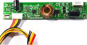
Special material circuit boards are used across a wide range of advanced electronic systems.
Industrial Electronics
Industrial control systems can require high reliability, stable thermal performance, and resistance to demanding operating conditions.
Special materials may be selected for motor control, industrial communication, power electronics, or high-temperature applications.
Medical Electronics
Medical equipment can require highly reliable electronic assemblies with controlled electrical and thermal performance.
Depending on the equipment architecture, special PCB materials may be used for high-speed data processing, imaging systems, power circuits, or compact electronic modules.
Material and process selection should be based on the complete device design and applicable regulatory requirements.
Automotive Electronics
Automotive electronic systems can experience temperature changes, vibration, electrical noise, and space constraints.
Special PCB materials and constructions may be used in:
- Power control systems
- Automotive communication
- ADAS electronics
- Infotainment
- Battery systems
- Motor control
High-Frequency Communication
RF and microwave systems require careful management of dielectric properties, conductor geometry, impedance, and signal loss.
Special low-loss materials can therefore be an important part of high-frequency PCB design.
Power Electronics
Power systems can require thicker copper, improved thermal paths, and mechanically robust PCB constructions.
Heavy copper and metal-core technologies may be considered depending on the electrical and thermal requirements.
Components and Material Supply Chain Management
Special material PCB projects can involve materials and components with longer lead times or fewer approved alternatives than standard PCB products.
Supply-chain planning should therefore begin early.
Important considerations include:
- Material availability
- Approved material alternatives
- Component lifecycle
- Lead times
- Minimum order quantities
- Material traceability
- Production continuity
For turnkey projects, Components Procurement can be coordinated with PCB fabrication and assembly to reduce scheduling risks and improve production planning.
Early procurement planning is particularly useful for projects using specialized laminates, uncommon components, or application-specific materials.
Designing Special Material PCBs for Manufacturability
Design for manufacturability should be incorporated into the project before PCB fabrication begins.
Important DFM considerations include:
- Material availability
- Stackup structure
- Minimum trace width
- Minimum spacing
- Copper thickness
- Via dimensions
- Drill specifications
- Lamination requirements
- Surface finish
- Component clearance
- Mechanical features
- Panelization
- Testing requirements
A PCB design may be technically feasible but difficult or expensive to manufacture consistently.
Early communication between the designer and manufacturer can identify potential problems before production.
For complex boards, reviewing the fabrication strategy together with the PCB Manufacturing process can help optimize material selection, stackup construction, tolerances, and production efficiency.
How to Choose a Special Material PCB Manufacturing Partner
Selecting a suitable manufacturing partner is an important decision for demanding PCB projects.
Key evaluation criteria should include:
Material Experience
The manufacturer should understand the specific materials used in the project and their fabrication characteristics.
Process Capability
The supplier should have appropriate capabilities for:
- Precision drilling
- Fine-line fabrication
- Heavy copper
- HDI
- Flexible or rigid-flex PCB
- Controlled impedance
- Special surface finishes
- Advanced inspection
Engineering Support
Engineering support is valuable when material compatibility, stackup construction, or manufacturing tolerances require optimization.
Quality Control
A structured quality system should cover raw materials, fabrication processes, electrical testing, dimensional inspection, and final product verification.
Assembly Capability
If the project requires both bare PCB fabrication and component assembly, an integrated manufacturing workflow can simplify communication and production management.
Future Trends in Special Material PCB Manufacturing
As electronic systems become faster, smaller, and more power-intensive, demand for specialized PCB materials is likely to continue increasing.
Important development trends include:
- Lower-loss high-frequency materials
- Higher-density interconnection
- More advanced hybrid material structures
- Thicker copper constructions
- Improved thermal management
- Flexible and rigid-flex integration
- Advanced surface finishes
- More precise manufacturing processes
- Greater automation and inspection
- Increasingly integrated PCB assembly
The boundary between PCB manufacturing, semiconductor packaging, thermal engineering, and advanced electronics is becoming increasingly interconnected.
Manufacturers will therefore need to combine material knowledge with precision fabrication, process engineering, and assembly expertise.
Why Special Material PCB Quality Matters
A Special Material PCB is often selected because standard PCB materials cannot fully satisfy the electrical, thermal, mechanical, or environmental requirements of the application.
However, using a high-performance material does not automatically guarantee high PCB performance.
The final result depends on the complete manufacturing chain, including:
- Material selection
- Stackup design
- Lamination
- Drilling
- Etching
- Plating
- Impedance control
- Surface finishing
- Inspection
- PCB assembly
- Testing
A well-designed manufacturing process ensures that the selected material’s properties are translated into reliable finished-board performance.
For demanding electronics, manufacturing capability and engineering support should therefore be evaluated as carefully as the material itself.
Conclusion
Special Material PCB Manufacturing requires a combination of advanced materials, precise fabrication processes, controlled manufacturing parameters, and comprehensive quality management.
Whether the application involves high-frequency communication, high-current power systems, flexible electronics, industrial equipment, medical devices, or automotive electronics, the PCB material must be matched carefully to the system’s electrical, thermal, mechanical, and environmental requirements.
Successful production also depends on precision drilling, controlled impedance, reliable lamination, appropriate surface finishes, high-quality PCB assembly, and comprehensive testing.
By integrating material selection, PCB design, manufacturing engineering, prototype validation, component procurement, and quality control into one structured process, engineers can reduce production risks and build more reliable electronic products.
As electronic systems continue to demand higher frequencies, greater power density, smaller form factors, and more complex functionality, Special Material PCB technology will remain an important foundation for next-generation electronic manufacturing.