1oz Copper PCB 4-Layer Controlled Impedance PCB for High-Speed Electronic Applications
In modern electronic systems, PCBs serve as the essential platform for component connection, signal transmission, and power distribution. Among various PCB solutions, the 4-Layer Impedance PCB with 1oz copper thickness has become an important choice for communication equipment, computing systems, automotive electronics, and industrial applications due to its balanced electrical performance, mechanical reliability, and manufacturing flexibility.
The combination of 1oz copper thickness and a four-layer structure provides an effective solution for applications requiring stable current carrying capability, controlled signal transmission, and compact circuit integration.
A properly designed Controlled Impedance PCB can maintain signal integrity by controlling trace geometry, dielectric characteristics, copper thickness, and layer arrangement. This makes it suitable for high-speed digital circuits, communication devices, and other electronic systems where signal quality is critical.
Understanding 1oz Copper 4-Layer Impedance PCB
Meaning of 1oz Copper Thickness
In PCB manufacturing, “oz” represents the weight of copper over an area of one square foot. A 1oz copper layer corresponds to approximately 35μm copper thickness.
This copper thickness is one of the most commonly used specifications because it provides a good balance between electrical conductivity, mechanical strength, manufacturability, and cost efficiency.
A thicker copper layer reduces conductor resistance and improves current-carrying capability. Similar to a wider highway allowing more vehicles to pass smoothly, copper layers with sufficient thickness allow electrical current to flow more efficiently while reducing power loss and heat generation.
In power distribution circuits, 1oz copper traces can support higher current requirements while improving reliability and reducing the risk of excessive temperature rise.
Four-Layer PCB Structure
A typical four-layer impedance-controlled PCB consists of:
- Top signal layer
- Inner power layer
- Inner ground layer
- Bottom signal layer
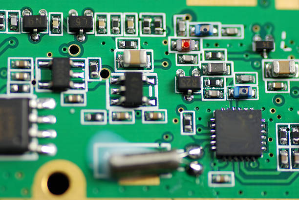
The top and bottom layers are generally used for component placement and signal routing. Semiconductor devices, resistors, capacitors, connectors, and other electronic components are mounted on these external layers.
The internal power layer provides stable voltage distribution throughout the circuit, while the ground layer creates a low-impedance return path and helps reduce electromagnetic interference.
These layers are electrically connected through vias, allowing signals and power to transfer between different sections of the board.
For advanced multilayer structures, proper stack-up planning is essential. More information can be found in Multilayer PCB Manufacturing.
Importance of Controlled Impedance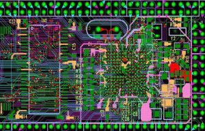
Impedance refers to the resistance of a circuit to alternating current signals. For high-frequency and high-speed transmission, maintaining consistent impedance is essential for preserving signal integrity.
In a High-Speed PCB design, impedance values such as 50Ω and 75Ω are commonly used depending on the application requirements.
By accurately controlling trace width, copper thickness, dielectric thickness, and dielectric constant, manufacturers can achieve the required impedance values.
When source impedance, transmission-line impedance, and load impedance are properly matched, signals can travel with minimal reflection and distortion.
This prevents issues such as:
- Signal attenuation
- Data errors
- Crosstalk
- Reflection loss
- Timing instability
For high-speed applications, impedance control is not only a design requirement but also a manufacturing capability that requires precise process management.
Manufacturing Process Requirements
Material Selection
PCB Substrate Materials
FR-4 is one of the most commonly used materials for 1oz copper four-layer PCBs because of its excellent electrical insulation properties, mechanical strength, thermal stability, and dimensional reliability.
For applications requiring higher frequency performance, specialized low-loss materials may be selected to improve signal transmission quality.
High-frequency materials with lower dielectric loss help reduce signal attenuation and improve impedance consistency in demanding communication applications.
Copper Foil Selection
During manufacturing, copper foil thickness must be carefully controlled to achieve the final 1oz copper specification.
Manufacturers may begin with thinner copper foil, such as 1/3oz or 1/2oz copper, and increase the final copper thickness through electroplating processes.
This approach provides better control during circuit formation while ensuring the finished PCB meets electrical and reliability requirements.
Circuit Fabrication Technology
High-Precision Circuit Formation
Controlled impedance applications require accurate trace geometry. Advanced imaging and etching technologies help achieve precise line width, spacing, and conductor profiles.
For a typical 50Ω transmission line design, manufacturers must accurately control:
- Trace width
- Trace spacing
- Copper thickness
- Dielectric thickness
- Distance to reference planes
These parameters directly influence impedance performance.
High-precision manufacturing reduces impedance variation, minimizes signal reflection, and improves transmission efficiency.
For advanced impedance design solutions, see PCB Impedance Control Design.
Microvia and Via Processing
Although four-layer boards have fewer layers than high-density multilayer designs, reliable via processing remains important for electrical connection and signal performance.
Laser drilling technology can be used for microvia structures in advanced designs requiring higher routing density.
High-quality via manufacturing requires:
- Accurate drilling position
- Smooth hole walls
- Reliable copper plating
- Controlled aspect ratio
Proper via design reduces signal discontinuity and improves long-term electrical reliability.
Surface Finishing Technology
Surface finishing protects exposed copper areas and provides reliable soldering performance.
ENIG (Electroless Nickel Immersion Gold) is widely used because it provides:
- Excellent solderability
- Corrosion resistance
- Stable electrical contact
- Good surface flatness
For RF interfaces and precision electronic assemblies, surface finish quality can influence connection reliability and signal performance.
A suitable surface treatment helps reduce contact resistance and maintain stable electrical connections.
Performance Advantages
Excellent Electrical Performance
The 1oz copper layer provides lower conductor resistance and improves current transmission efficiency.
In communication equipment, reduced resistance helps minimize signal loss and maintain signal quality during transmission.
The four-layer structure combined with controlled impedance design creates a stable transmission environment for high-speed signals.
This makes it suitable for applications such as networking equipment, communication modules, and high-speed electronic systems.
For advanced communication PCB solutions, see High Frequency PCB Manufacturing.
Strong Mechanical Reliability
The combination of FR-4 substrate materials and 1oz copper thickness provides good mechanical stability.
This allows the PCB to withstand vibration, mechanical stress, and environmental changes.
In automotive electronics, for example, electronic systems are exposed to continuous vibration and temperature fluctuations. A reliable 1oz copper four-layer impedance PCB can support applications such as:
- Engine control systems
- Vehicle infotainment systems
- Electronic control modules
Effective Thermal Management
Electronic components generate heat during operation, making thermal management essential for system reliability.
The copper layer itself acts as a thermal pathway, transferring heat away from high-power components.
The four-layer structure also allows designers to use large copper areas on power and ground layers to improve heat spreading.
Combined with thermal vias and external cooling structures, the PCB can maintain stable operating temperatures during long-term high-load operation.
Application Fields
Communication Applications
1oz copper four-layer impedance PCBs are widely used in:
- 5G communication equipment
- Routers
- Network switches
- Wireless modules
Communication systems require stable signal transmission and controlled electrical characteristics.
The impedance-controlled structure helps maintain high-speed data transmission while reducing signal distortion.
For advanced communication hardware development, High-Speed PCB Prototyping provides additional information about high-speed PCB design and manufacturing.
Computer Systems
Computer motherboards require reliable power distribution and high-speed communication between processors, memory, storage devices, and peripheral interfaces.
A 1oz copper four-layer impedance PCB can provide:
- Stable power delivery
- Reliable signal routing
- Improved electrical performance
In servers and computing platforms, controlled impedance design helps maintain data integrity for high-speed interfaces and complex digital systems.
Automotive Electronics
With the development of intelligent vehicles and electric vehicles, automotive electronic systems are becoming increasingly complex.
1oz copper four-layer impedance PCBs are used in:
- Autonomous driving systems
- Battery management systems
- Vehicle communication systems
- Infotainment systems
These applications require reliable signal transmission, mechanical stability, and resistance to challenging operating environments.
Medical Equipment
Medical imaging systems such as MRI and CT scanners require highly reliable electronic circuits for precise signal processing.
The electrical stability and controlled transmission characteristics of 1oz copper four-layer impedance PCBs make them suitable for medical applications requiring accurate data acquisition and signal processing.
In MRI systems, for example, PCB assemblies help manage RF signal transmission and control circuits, contributing to accurate imaging performance.
Conclusion
The 1oz Copper PCB with a four-layer controlled impedance structure provides an excellent balance of electrical performance, mechanical reliability, thermal capability, and manufacturing efficiency.
Through precise material selection, impedance control, advanced circuit fabrication, reliable via processing, and quality surface finishing, this type of PCB supports a wide range of modern electronic applications.
As electronic devices continue moving toward higher speeds, greater integration, and more complex functions, the combination of 1oz Copper PCB, 4-Layer Impedance PCB, Controlled Impedance PCB, Multilayer PCB, and High-Speed PCB technologies will continue playing an important role in the development of next-generation electronic systems.