Multilayer High-Speed PCB Prototyping for Server Motherboards
SEO Description: Learn how multilayer high-speed PCB prototyping supports server motherboards through advanced stack-up design, material selection, impedance control, precision fabrication, and comprehensive testing.
SEO Keywords: Multilayer High-Speed PCB, Server Motherboard PCB, High-Speed PCB Prototyping, Controlled Impedance PCB, High-Frequency PCB
Server hardware relies heavily on the motherboard as the central interconnection platform. It must support high-speed signal transmission, multiple power rails, high-density routing, thermal management, and operation in a complex electromagnetic environment. As a result, a Multilayer High-Speed PCB has become an important foundation for modern server motherboards.
With carefully engineered layer structures, high-quality materials, controlled impedance, and precise manufacturing, multilayer PCBs can provide the electrical and mechanical performance required by demanding server applications. Prototyping is an essential step before mass production because it allows engineers to validate the PCB structure, identify potential manufacturing problems, and optimize electrical performance before committing to large-scale production.
GOPCBA provides PCB Manufacturing Services covering multilayer, HDI, high-speed, controlled-impedance, blind and buried via, and other advanced PCB technologies.
Server motherboards must support multiple high-speed interfaces, processors, memory devices, storage interfaces, power-management circuits, and communication channels within a relatively limited PCB area. Conventional low-layer-count boards often cannot provide sufficient routing capacity, power distribution, signal isolation, and electromagnetic control.
A Server Motherboard PCB with a multilayer architecture can provide several important advantages.
First, it improves high-speed signal transmission. By carefully arranging signal layers and continuous reference planes, engineers can create more predictable transmission paths and reduce signal reflection, crosstalk, and electromagnetic interference.
Second, multilayer construction improves power distribution. Server processors, memory systems, networking devices, and other high-performance components may require multiple voltage rails. Dedicated power and ground planes can create lower-impedance current paths and help reduce power-distribution noise.
Third, multilayer structures improve electromagnetic compatibility. Ground planes positioned close to signal layers can reduce the loop area of high-frequency currents and help contain electromagnetic radiation. This is particularly important in servers containing multiple high-speed interfaces and densely packed electronic components.
For advanced server designs, the appropriate layer count depends on routing density, signal speed, power requirements, mechanical dimensions, thermal requirements, and manufacturing constraints.
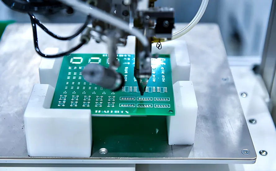
The quality of the prototype directly affects the reliability of the final server motherboard. Therefore, High-Speed PCB Prototyping should focus on stack-up design, material selection, precision drilling, lamination, impedance control, and inspection.
Stack-up design is one of the most important factors in high-speed multilayer PCB development. The number and arrangement of signal, ground, and power layers should be determined according to the electrical architecture of the server motherboard.
High-speed signal layers should generally have continuous reference planes to maintain a predictable return-current path. The distance between the signal layer and reference plane also affects transmission-line impedance.
For demanding designs, the stack-up should be established before final routing rather than being treated as a manufacturing detail afterward. A properly engineered stack-up helps coordinate trace width, copper thickness, dielectric thickness, material properties, and target impedance.
GOPCBA’s High-Speed PCB Stack-Up Design guidance explains how layer arrangement, reference planes, and impedance control should be considered together during high-speed PCB development.
Material selection is equally important. Server motherboards operating at high data rates may require materials with stable dielectric properties, low dielectric loss, good thermal performance, and appropriate dimensional stability.
For particularly demanding applications, a High-Frequency PCB material system may be considered to reduce transmission loss and maintain stable electrical characteristics across the required frequency range.
Multilayer server PCBs rely on through vias, blind vias, buried vias, and, in some designs, microvias to establish electrical connections between different layers.
Drilling accuracy is therefore critical. Variations in hole diameter, hole position, annular ring dimensions, and layer registration can affect electrical connectivity, manufacturing yield, and high-speed performance.
For high-density designs, via spacing must also be carefully controlled. Vias positioned too close to one another or too close to traces and pads can create manufacturing difficulties during drilling, plating, and layer alignment.
GOPCBA’s Multilayer PCB Via Spacing Guide provides additional guidance on hole-to-hole and hole-to-trace spacing for multilayer PCB layouts.
Lamination is another critical manufacturing stage. High-layer-count PCBs typically require precise control of temperature, pressure, vacuum, and lamination time. Proper process control helps prevent voids, delamination, uneven dielectric thickness, and layer misalignment.
Stable dielectric thickness is particularly important for high-speed transmission lines because changes in the distance between a trace and its reference plane can alter the characteristic impedance.
During prototype manufacturing, the external and internal circuit patterns must be formed with high dimensional accuracy.
Processes such as cleaning, photoresist application, exposure, development, etching, and copper plating directly influence trace width, spacing, copper thickness, and conductor geometry.
For high-speed server motherboards, small deviations in trace geometry can affect impedance and signal performance. Manufacturers therefore need to maintain consistent imaging and etching conditions throughout production.
Copper thickness should also be selected according to the electrical and thermal requirements of each layer. Power and high-current layers may require heavier copper, while high-speed signal layers often require carefully controlled conductor dimensions to maintain the required impedance.
Surface finishing should be selected according to the PCB’s electrical, mechanical, and assembly requirements. Common options include ENIG, HASL, OSP, immersion tin, immersion silver, and other specialized finishes.
The surface finish should provide reliable solderability and corrosion resistance without compromising the requirements of the intended application.
The primary purpose of PCB prototyping is not simply to produce a physical sample. It is to verify whether the design and manufacturing process can meet the required electrical, mechanical, and reliability targets before mass production.
For a Controlled Impedance PCB, impedance verification is particularly important.
High-speed server interfaces rely on predictable transmission-line characteristics. If the actual impedance differs significantly from the design target, signal reflections and waveform distortion may occur.
TDR testing can be used to evaluate impedance along a transmission path and identify discontinuities associated with traces, vias, connectors, or layer transitions.
The impedance result can then be compared with the target defined during stack-up and layout development. If deviations are identified, engineers can investigate factors such as trace width, copper thickness, dielectric thickness, material Dk, reference-plane distance, or manufacturing variation.
GOPCBA’s High-Frequency Multilayer PCB manufacturing guidance also highlights the relationship between trace geometry, dielectric properties, stack-up structure, copper characteristics, and controlled impedance.
A complete prototype verification process should include more than impedance testing.
AOI inspection can be used to identify defects in internal and external circuit patterns, including opens, shorts, missing features, excessive copper, and pattern deviations.
Electrical testing can verify circuit continuity and isolation. For complex multilayer structures, X-ray inspection can provide additional information about internal alignment, via structures, and potential manufacturing defects.
These inspections are especially valuable for server motherboard prototypes because a manufacturing defect discovered after assembly can significantly increase debugging time and development costs.
Before fabrication begins, the design files should undergo a detailed manufacturability review.
Important parameters include:
GOPCBA supports engineering review and DFM analysis as part of its PCB manufacturing workflow, helping identify potential production risks before fabrication.
High-Speed PCB Prototyping serves as an important bridge between PCB design and volume manufacturing.
A prototype allows engineers to validate the stack-up, signal paths, power distribution, thermal behavior, mechanical dimensions, and manufacturing process before production quantities increase.
During this stage, engineers may discover issues such as impedance deviation, insufficient routing space, excessive crosstalk, thermal concentration, poor via placement, or manufacturing limitations.
These problems can then be corrected before mass production, reducing the risk of expensive redesigns and production failures.
GOPCBA’s Rapid PCB Prototyping service is designed to support prototype development and testing before production. The company describes rapid prototyping as a way to validate PCB designs, identify problems, and make modifications before mass manufacturing.
The development of AI servers and high-performance computing platforms places even greater demands on PCB technology.
Modern server platforms may combine high-performance processors, GPUs, high-speed memory, networking interfaces, storage devices, and high-current power delivery within a compact system.
This increases requirements for:
For these systems, high-layer-count PCBs can provide additional routing resources and dedicated reference and power planes. However, increasing the number of layers also makes stack-up design, lamination, layer registration, drilling, and inspection more demanding.
Therefore, prototype validation becomes even more important before entering volume production.
A well-developed prototype can help engineers confirm whether the selected materials and stack-up can support the required electrical and thermal performance under realistic operating conditions.
The development of a reliable server motherboard PCB should not treat design, prototyping, manufacturing, and testing as isolated activities.
A more effective workflow is: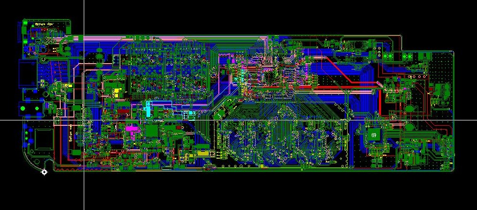
Design → Stack-Up Engineering → Material Selection → DFM Review → Prototype Fabrication → Inspection → Electrical Testing → Performance Validation → Design Optimization → Mass Production
This integrated approach allows engineering teams to identify problems earlier and establish a more stable production process.
Manufacturing data collected during prototyping can also be used to optimize mass-production parameters. For example, impedance measurements can help verify whether the selected trace geometry and dielectric structure are appropriate, while inspection results can identify recurring registration or drilling issues.
The prototype therefore becomes both a physical validation sample and a source of manufacturing data for subsequent production.
Multilayer high-speed PCB prototyping is a critical stage in the development of modern server motherboards. A reliable Server Motherboard PCB must simultaneously support high-speed signal transmission, complex power distribution, high-density interconnection, thermal management, and electromagnetic compatibility.
Achieving these requirements depends on more than simply increasing the PCB layer count. Stack-up design, material selection, impedance control, precision drilling, lamination, circuit fabrication, inspection, and electrical testing must all work together.
For demanding server and AI computing applications, Multilayer High-Speed PCB, High-Speed PCB Prototyping, Controlled Impedance PCB, and High-Frequency PCB technologies provide the foundation for reliable signal transmission and stable system operation.
By validating these critical factors during the prototype stage, engineers can identify design and manufacturing risks earlier, optimize the PCB structure, improve production yield, and establish a more reliable path from prototype development to mass production.