How to Repair Broken PCB Traces: PCB Repair, Troubleshooting & Trace Repair Guide
Modern electronics continue to become smaller, lighter, more powerful, and more affordable. Inside these products are increasingly dense electronic circuits mounted on dielectric substrates known as printed circuit boards (PCBs).
As circuit density increases, the possibility of PCB failures also increases. A failure may result from a manufacturing defect, an incorrect
, mechanical stress, overheating, corrosion, improper handling, or damage during operation. One common problem is a broken or damaged PCB trace, which can interrupt an electrical connection and cause the entire device or circuit to malfunction.
So, how do you repair a broken PCB trace?
PCB trace repair is a common PCB repair technique used to restore electrical continuity after a copper trace has cracked, lifted, burned, or been physically damaged. Depending on the location and severity of the damage, a repair may involve soldering a jumper wire, rebuilding a section of copper, or using specialized PCB repair materials.
This guide explains what PCB traces are, how to diagnose damaged traces, which tools are required, how to repair broken PCB traces, and what precautions should be taken to achieve a reliable repair.
Featured Snippet Answer: To repair a broken PCB trace, first disconnect power and inspect the damaged area under magnification. Use a multimeter to confirm the open circuit, carefully remove solder mask from the intact copper on both sides of the break, apply flux, and bridge the damaged section with a suitable jumper wire or copper repair material. Secure and insulate the repair, then retest continuity and the circuit’s functionality before returning the PCB to service.
What Is a PCB Trace?
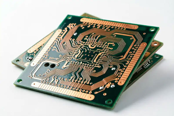
A PCB trace is a conductive pathway on a printed circuit board that electrically connects components, pads, vias, and other circuit features.
PCB traces are typically made from copper because copper offers:
- Excellent electrical conductivity
- Good thermal conductivity
- Relatively low cost
- Good manufacturability
- Long-term availability
Depending on the PCB structure, copper traces can exist on the outer layers or internal layers of the board.
Important PCB trace design parameters include:
- Trace width
- Trace length
- Copper thickness
- Trace spacing
- Current capacity
- Impedance
- Temperature rise
These parameters must be carefully considered during PCB Design because they directly affect current-carrying capability, voltage drop, thermal performance, signal integrity, and electromagnetic interference (EMI).
A trace carrying a high current generally requires more copper cross-sectional area than a low-current signal trace. High-speed and RF circuits may also require controlled impedance and carefully designed return paths.
What Causes Broken PCB Traces?
Before learning how to repair broken PCB traces, it is important to understand why traces fail.
Common causes include:
Mechanical Damage
A PCB may be damaged by:
- Bending
- Impact
- Dropping
- Excessive vibration
- Incorrect handling
- Improper connector insertion or removal
Mechanical stress can crack copper traces or cause them to separate from the substrate.
Overheating
Excessive current or heat can damage copper traces, solder joints, and nearby components.
A severely overloaded trace may become discolored, burned, or physically open.
Manufacturing Defects
PCB manufacturing problems can also result in defective traces.
Examples include:
- Incomplete etching
- Over-etching
- Insufficient copper
- Poor plating
- Surface contamination
- Lamination-related damage
Reliable PCB Manufacturing processes and inspection help reduce these risks.
Corrosion
Moisture, chemicals, contaminants, and unsuitable environmental conditions can corrode exposed copper and eventually interrupt electrical connections.
Component or Soldering Damage
Excessive soldering temperature, repeated rework, or mechanical stress during component removal can lift pads and damage nearby traces.
How Do You Diagnose a Broken PCB Trace?
The first step in PCB Troubleshooting is determining whether the trace is actually broken.
Modern PCBs can contain very narrow traces and closely spaced components, making visual diagnosis difficult. A combination of visual inspection and electrical testing is therefore recommended.
1. Perform a Visual Inspection
Start by disconnecting the PCB from all power sources.
Inspect the board under good lighting and look for:
- Cracked traces
- Burn marks
- Scratched copper
- Lifted pads
- Delamination
- Discoloration
- Solder bridges
- Corrosion
- Physical cracks in the PCB
A magnifying glass can help with larger boards, while a microscope may be necessary for fine-pitch or high-density PCBs.
Pay particular attention to areas around connectors, mounting holes, power components, and locations that may have experienced mechanical stress.
2. Use a Multimeter
A digital multimeter is one of the most useful tools for PCB Testing and trace diagnosis.
With the PCB unpowered, use continuity or resistance mode to test the suspected trace.
Place one probe on one intact section of the trace and the other probe on the other side of the suspected break.
A properly connected trace should normally show continuity or a low resistance appropriate to the circuit. An open circuit suggests that the conductive path has been interrupted.
However, in-circuit measurements can sometimes be affected by other components connected to the same electrical network. If the measurement is ambiguous, isolate the relevant section or compare it with the schematic.
3. Use Advanced PCB Inspection Methods
For complex or multilayer boards, advanced diagnostic equipment may be necessary.
AOI
Automated Optical Inspection (AOI) uses high-resolution imaging to identify visible PCB defects.
AOI can help detect:
- Trace defects
- Missing copper features
- Solder bridges
- Component placement problems
- Manufacturing anomalies
X-Ray Inspection
X-ray inspection can identify internal PCB problems that cannot be seen from the surface.
This can be particularly useful for multilayer boards or assemblies containing hidden solder joints and internal structures.
TDR Testing
A Time-Domain Reflectometer (TDR) sends a high-speed electrical signal through a conductive path and analyzes reflections caused by impedance changes.
For suitable controlled-impedance structures, TDR can help locate discontinuities or damage along a trace or interconnect.
For ordinary low-speed PCB repairs, however, a multimeter and visual inspection are usually sufficient.
What Tools and Materials Are Needed for PCB Trace Repair?
The tools required depend on the severity and location of the damage.
Basic PCB Repair work may require:
- Temperature-controlled soldering iron
- Fine soldering tip
- Solder wire
- Flux
- Digital multimeter
- Magnifying glass or microscope
- Fine tweezers
- Precision knife or fiberglass scratch pen
- Fine-gauge insulated wire
- PCB repair wire
- Epoxy or suitable PCB repair material
- Isopropyl alcohol and cleaning materials
- Kapton or other heat-resistant tape
For professional repair work, additional equipment may include:
- Hot-air rework station
- Microscope
- PCB preheater
- PCB holder
- ESD-safe workstation
- Thermal camera
- Specialized PCB trace repair kits
Always use appropriate ESD protection when working with sensitive electronic components.
How to Repair a Broken PCB Trace
There are several ways to repair a damaged PCB trace. The correct method depends on the size of the break, current requirements, PCB layer structure, accessibility, and reliability requirements.
For many prototype and repair applications, a jumper-wire repair is the simplest approach.
Method 1: Repair a Broken PCB Trace With a Jumper Wire
A jumper wire can bypass the damaged section and restore electrical continuity.
Step 1: Confirm the Damage
Use a multimeter to confirm that the suspected trace is actually open.
Refer to the schematic or PCB layout to identify both electrical endpoints of the damaged trace.
Step 2: Disconnect Power
Make sure the PCB is completely disconnected from all power sources.
If the board contains batteries or other energy-storage components, follow appropriate discharge procedures before working on it.
Step 3: Clean the Damaged Area
Clean the PCB surface to remove dirt, oxidation, flux residue, or other contaminants.
Isopropyl alcohol can often be used for general PCB cleaning when it is compatible with the board and components.
Allow the area to dry completely.
Step 4: Expose Intact Copper
Use a fiberglass pen or an appropriate precision tool to carefully remove a small amount of solder mask from the intact copper on both sides of the damaged section.
Do not remove more solder mask than necessary.
The goal is to expose enough clean copper to create reliable solder joints without damaging neighboring traces or the PCB substrate.
Step 5: Apply Flux and Pre-Tin the Copper
Apply a small amount of flux to the exposed copper.
Pre-tin the exposed areas with a small amount of solder.
Avoid excessive solder because large solder masses can create unwanted connections to adjacent conductors.
Step 6: Prepare the Jumper Wire
Select a wire with an appropriate diameter and insulation for the circuit.
The wire must be capable of carrying the required current and withstand the electrical and environmental conditions of the application.
For low-current signal traces, a fine insulated wire may be appropriate. Higher-current applications may require a larger conductor or a more substantial copper repair.
Step 7: Solder the Jumper
Solder one end of the jumper wire to the exposed copper on one side of the broken trace.
Route the wire carefully and solder the other end to the intact copper on the opposite side.
Keep the repair as short as practical and secure the wire so that it cannot move excessively.
Step 8: Secure the Repair
After confirming the electrical connection, mechanically secure the repaired wire using an appropriate insulating or bonding material.
For suitable applications, epoxy or another PCB-compatible material can help prevent mechanical movement.
Do not allow adhesive to interfere with connectors, moving parts, heat-generating components, or future service points.
Step 9: Test the Repair
Use a multimeter to verify continuity across the repaired section.
Then check for unintended connections between the repaired trace and nearby conductors.
Finally, perform functional testing of the circuit.
This final verification is an essential part of reliable PCB Troubleshooting.
Method 2: Rebuild the Damaged Trace
For some repairs, especially where maintaining the original geometry is important, the damaged copper trace can be rebuilt rather than bypassed with a wire.
A specialized PCB trace repair kit may include replacement copper foil or conductive repair material.
The general process involves:
- Cleaning the damaged area.
- Removing loose or severely damaged copper.
- Exposing intact copper at both ends of the damaged section.
- Preparing a replacement copper strip or suitable repair material.
- Aligning the replacement conductor with the original trace.
- Bonding or soldering the replacement conductor as appropriate.
- Securing the repair mechanically.
- Testing electrical continuity and isolation.
This method requires greater precision than a simple jumper-wire repair and may be more appropriate for professional PCB Repair work.
Repairing Lifted PCB Pads
A broken trace may sometimes be accompanied by a lifted or damaged solder pad.
In this situation, simply soldering a jumper wire to the damaged pad may not provide a mechanically reliable connection.
The repair may require:
- Exposing a suitable section of intact trace
- Creating a new connection point
- Installing a replacement pad or copper foil
- Bonding the repaired structure
- Reinforcing the area
- Performing electrical and mechanical inspection
Fine-pitch and high-density boards should generally be repaired under magnification.
Repairing Internal or Multilayer PCB Traces
Repairing an internal trace on a multilayer PCB is significantly more difficult than repairing an accessible surface trace.
Because internal copper layers cannot normally be accessed directly from the surface, the repair may require specialized techniques and equipment.
Possible approaches include:
- Controlled PCB layer excavation
- Micro-drilling
- Specialized jumper connections
- Via repair
- Conductive materials
- Professional PCB rework techniques
If the damaged board is expensive, safety-critical, multilayer, or difficult to replace, professional PCB repair services may be more appropriate than attempting an improvised repair.
Important Guidelines for PCB Trace Repair
Following good repair practices helps prevent additional damage.
Match the Electrical Capability
The replacement conductor should be appropriate for the original circuit.
Consider:
- Current
- Voltage
- Trace width
- Copper thickness
- Temperature
- Signal frequency
- Impedance requirements
A very thin jumper wire may work for a low-current signal but may be unsuitable for a power trace.
Keep Repair Length Short
Where practical, keep the repair path short.
Longer wires can introduce additional resistance, inductance, capacitance, and electromagnetic coupling, which may be important in high-speed, RF, or sensitive analog circuits.
Avoid Excessive Heat
Excessive soldering temperature or prolonged heating can damage:
- PCB substrate
- Copper traces
- Solder pads
- Nearby components
- Solder mask
Use a temperature-controlled soldering station and work efficiently.
Protect Adjacent Traces
High-density PCB layouts can contain extremely narrow clearances.
Use magnification and avoid accidentally scratching or lifting neighboring traces while removing solder mask.
Maintain ESD Protection
Sensitive ICs, microcontrollers, memory devices, sensors, and RF components can be damaged by electrostatic discharge even when there is no visible damage.
Use an ESD-safe workstation when appropriate.
Test Before and After Repair
Measure the circuit before repair to establish the fault.
After repair, verify:
- Continuity
- Isolation from adjacent conductors
- Power-rail behavior
- Component voltages
- Functional operation
Do not assume that a repaired trace is successful simply because it looks correct.
When Should a PCB Be Repaired or Replaced?
Not every damaged PCB should be repaired.
PCB repair may be worthwhile when:
- The board is expensive
- Replacement boards are unavailable
- The damage is localized
- The PCB contains proprietary components
- The product is obsolete
- A prototype needs to be restored
- The board can be safely reworked
Replacement may be preferable when:
- The PCB has extensive burn damage
- Multiple internal layers are damaged
- The substrate is severely delaminated
- Critical safety functions are affected
- The repair cannot meet the original reliability requirements
- The cost of repair approaches the cost of replacement
For safety-critical, medical, automotive, aerospace, or high-reliability electronics, repair decisions should follow the applicable quality and engineering procedures.
Common PCB Trace Repair Mistakes
Using Wire That Is Too Thin
A wire that cannot safely carry the required current can overheat or fail.
Applying Too Much Solder
Excessive solder can bridge adjacent pads or traces and create a new short circuit.
Scratching Too Deeply
Aggressive scraping can damage the substrate or neighboring copper features.
Applying Excessive Heat
Long exposure to heat can lift pads and damage components.
Failing to Secure the Jumper
An unsecured wire can move, fatigue, or detach during vibration and handling.
Skipping the Final Test
A visual inspection alone cannot confirm that the repair is electrically correct.
How Kingda Can Support PCB Troubleshooting and Manufacturing
When a PCB has a damaged trace, the repair process should begin with accurate fault diagnosis rather than immediately replacing or soldering components.
Kingda can support projects involving PCB Manufacturing, PCB Assembly, and PCB-related troubleshooting requirements, depending on the specific project and service scope.
For production applications, prevention is often better than repair. Proper PCB Design, manufacturing controls, inspection, and electrical testing can reduce the risk of trace defects before the board reaches the end user.
When selecting a PCB manufacturing or repair partner, consider:
- PCB technology capabilities
- Layer count
- Material options
- Copper thickness
- Fine-line capabilities
- Inspection methods
- Electrical testing
- Assembly capabilities
- Rework and repair capabilities
- Quality control procedures
- Engineering support
A reliable manufacturing and engineering partner can help identify the root cause of PCB failures and determine whether repair, redesign, or replacement is the most appropriate solution.
Frequently Asked Questions About Repairing Broken PCB Traces
How do you repair a broken PCB trace?
First disconnect power and confirm the damaged trace with a multimeter. Expose a small amount of intact copper on both sides of the break, apply flux, and connect the two points with a suitable jumper wire or PCB repair material. Secure the repair and test continuity and circuit functionality afterward.
Can you repair a PCB trace with solder?
Solder alone is generally not an ideal replacement for a missing section of copper trace, particularly when the trace carries significant current or requires controlled electrical characteristics. A suitable jumper wire or copper repair material is normally a more reliable solution.
How do you find a broken trace on a PCB?
Start with visual inspection under magnification and then use a multimeter to check continuity between points along the suspected circuit path. For complex or multilayer boards, AOI, X-ray inspection, or TDR may help identify certain types of defects.
Can a burned PCB trace be repaired?
A burned trace can sometimes be repaired if the surrounding PCB substrate and other structures remain intact. The damaged copper should be assessed and removed as necessary before rebuilding the electrical connection with an appropriately sized conductor.
What wire should I use to repair a PCB trace?
The repair wire should have sufficient current capacity, suitable insulation, and appropriate mechanical and electrical properties for the application. Low-current signal traces can often use fine insulated wire, while power traces require a conductor sized for the expected current and temperature rise.
Can you repair a broken trace on a multilayer PCB?
Sometimes, but internal-layer damage is significantly more difficult to repair than an accessible outer-layer trace. Specialized PCB repair techniques may be required, and replacement can be preferable when reliability requirements are high.
How do you test a PCB trace with a multimeter?
With the PCB powered off, place the probes at two points that should be electrically connected. A properly connected trace should normally show continuity or a low resistance appropriate to the circuit. If no continuity is detected, inspect the trace and surrounding circuitry for an open connection.
Is it worth repairing a damaged PCB?
It depends on the board’s value, damage severity, availability of replacement boards, repair cost, and reliability requirements. Localized trace damage is often repairable, while extensive multilayer or substrate damage may make replacement more practical.
Conclusion
A broken PCB trace can prevent an otherwise functional electronic product from operating correctly. Fortunately, many localized trace failures can be diagnosed and repaired using appropriate PCB Testing, soldering techniques, jumper wires, and PCB repair materials.
The basic process is straightforward: identify the damaged trace, confirm the fault electrically, expose intact copper, restore the conductive path, secure the repair, and thoroughly test the board.
However, not every PCB trace should be repaired using the same technique. High-current circuits, high-speed signals, RF circuits, multilayer boards, fine-pitch assemblies, and safety-critical electronics may require specialized repair methods or professional evaluation.
Understanding how to repair broken PCB traces is therefore an important skill for engineers, technicians, students, and electronics hobbyists. At the same time, reliable PCB Design, PCB Manufacturing, PCB Assembly, and inspection processes remain the best ways to reduce PCB failures before they occur.