Multilayer PCB Inner Layer Lamination Sequence
The Multilayer PCB lamination sequence is a critical factor that determines the structural stability, electrical performance, and manufacturing yield of a circuit board. For complex products such as high-layer-count mixed-material PCBs and high-frequency high-speed PCBs, a properly designed inner layer lamination sequence ensures accurate layer alignment, reduces interlayer stress, and minimizes signal interference.
A well-planned stackup structure must consider electrical requirements, material characteristics, and manufacturing feasibility. The optimization of the PCB Layer Stackup process plays an essential role in achieving reliable performance for advanced electronic applications.
Key Factors for Planning PCB Inner Layer Lamination Sequence
The planning of a PCB Inner Layer Lamination sequence is not simply a matter of arranging layers in order. It must be based on circuit functionality, signal requirements, and mechanical considerations.
First, engineers need to define the role of each inner layer, including signal layers, ground layers, and power layers. The arrangement of these layers directly affects signal transmission paths and electromagnetic compatibility. For example, placing a high-speed signal layer between two ground layers creates a shielding structure that reduces electromagnetic radiation and improves signal integrity. This sandwich-style stackup is widely used in high-frequency and high-speed PCB designs.
The lamination sequence must also consider the thermal expansion characteristics of different materials. Various dielectric materials and copper foils have different coefficients of thermal expansion (CTE). If adjacent layers have significant differences in thermal expansion behavior, internal stress may develop during high-temperature lamination or long-term operation, potentially causing delamination or cracking.
For this reason, PCB manufacturers carefully select compatible materials and arrange layers with similar thermal characteristics together to achieve better stress balance. Advanced High Speed PCB manufacturing requires precise control of material combinations, dielectric thickness, and copper distribution.
In addition, the lamination sequence must match the manufacturing process. For complex multilayer boards, manufacturers often use a sequential lamination approach. Several inner-layer boards are first laminated into sub-assemblies, followed by secondary lamination with additional layers. This method improves layer registration accuracy and reduces thickness variation during production.
Critical Manufacturing Steps in Multilayer PCB Lamination
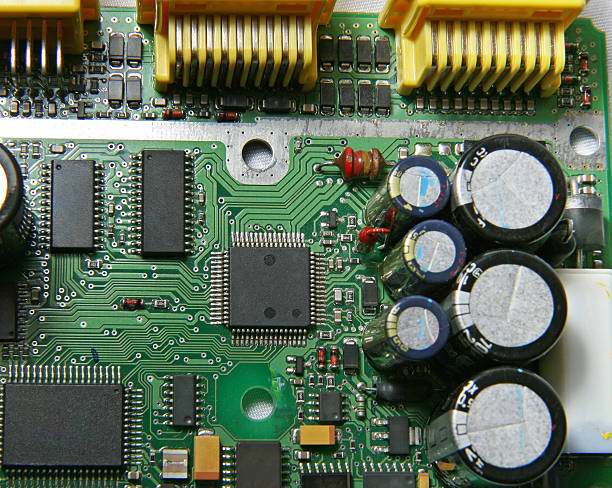
The implementation of the inner layer lamination sequence involves multiple key manufacturing procedures that directly influence final PCB quality.
Before lamination, inner layer preparation is essential. Each inner layer must undergo thorough cleaning and surface treatment to remove contaminants, oxidation, and residues. Proper surface preparation ensures strong bonding between copper layers and dielectric materials while preventing voids, bubbles, and poor adhesion.
Accurate registration is another important step. Alignment holes and positioning systems must be precisely controlled to ensure that all inner layers match correctly during stacking. Any registration error can result in circuit misalignment, affecting electrical connections and overall reliability.
During the stacking process, inner-layer circuit boards and prepreg materials are arranged according to the designed sequence. The selection and placement of prepreg materials are determined by bonding requirements, resin content, and curing characteristics.
The use of appropriate High Density Interconnect PCB technologies can further improve layer connectivity and routing capability in advanced multilayer PCB structures. Proper stacking control helps achieve finer line spacing, reliable microvia connections, and improved manufacturing consistency.
Cleanroom conditions are also required during stacking operations. Dust particles or foreign materials trapped between layers may cause defects after lamination. Operators must maintain strict process control to ensure uniform pressure distribution and consistent board thickness.
Lamination Parameter Control and Process Optimization
The lamination sequence works together with temperature, pressure, and curing time parameters. Different PCB structures require customized lamination profiles to achieve optimal bonding performance.
For example, multilayer PCBs containing heavy copper layers may require extended pressing time to ensure complete resin flow and strong copper-to-dielectric bonding. Temperature uniformity during the lamination cycle is equally important because uneven heating may degrade material properties and reduce long-term reliability.
Modern PCB manufacturing also relies on advanced testing methods, including impedance testing, cross-section analysis, and layer alignment inspection. These quality control procedures ensure that the final PCB Layer Stackup meets electrical and mechanical requirements.
A carefully optimized lamination process improves production stability, reduces manufacturing defects, and enhances the reliability of multilayer circuit boards used in demanding industries.
Impact of Lamination Sequence on PCB Performance
A properly designed lamination sequence significantly improves the overall performance of multilayer PCBs.
From a structural perspective, balanced layer arrangement helps distribute mechanical stress evenly and reduces board warpage. This is especially important for high-layer-count PCBs, where excessive thickness and complex structures can increase deformation risks during assembly and operation.
From an electrical perspective, the lamination sequence directly influences signal quality. By optimizing the relationship between signal layers, power planes, and ground planes, engineers can achieve better impedance control, lower transmission loss, and reduced crosstalk.
For high-speed electronic systems, placing reference planes close to signal layers provides stable return paths and improves signal integrity. Proper stackup design also supports thermal management by creating efficient heat dissipation paths.
The lamination structure is closely connected with other advanced manufacturing capabilities, including PCB Manufacturing Services, which provide customized solutions for complex multilayer circuit board production.
An improper lamination sequence may cause various reliability issues. Layer registration errors can lead to open circuits or short circuits. Uneven internal stress may result in delamination during thermal cycling. Poor signal layer arrangement can increase electromagnetic interference and reduce high-frequency transmission performance.
Therefore, optimizing the multilayer PCB lamination sequence is an important method for improving product reliability and competitiveness.
Advanced Lamination Technology for Reliable Multilayer PCB Production
The design and implementation of multilayer PCB inner layer lamination sequences require a combination of engineering expertise, material knowledge, and manufacturing experience.
For advanced applications, manufacturers must carefully evaluate PCB materials, copper thickness, layer distribution, and pressing parameters to achieve consistent quality. Technologies such as controlled impedance design, sequential lamination, and high-density routing are essential for producing next-generation electronic devices.
Professional PCB suppliers with advanced production capabilities can provide customized solutions for industries requiring high reliability, including telecommunications, automotive electronics, industrial control systems, and medical equipment.
Through continuous process optimization and strict quality management, PCB Prototype Services help customers validate complex PCB designs quickly while reducing development risks.
Reliable multilayer PCB manufacturing depends on precise lamination control, advanced fabrication technology, and comprehensive inspection processes. A scientifically optimized inner layer lamination sequence ensures stable electrical performance, excellent mechanical strength, and long-term operational reliability.
Conclusion
The multilayer PCB inner layer lamination sequence is one of the most important processes in advanced PCB manufacturing. It directly affects layer alignment, structural stability, signal integrity, thermal performance, and overall product reliability.
By combining optimized PCB Inner Layer Lamination techniques with advanced manufacturing capabilities, PCB manufacturers can deliver high-performance circuit boards that meet increasingly demanding application requirements.
With professional engineering support and advanced production technology, GOPCBA provides reliable multilayer PCB solutions for global customers, supporting applications that require precision, durability, and consistent performance through every stage of PCB development.
GOPCBA offers comprehensive solutions including Multilayer PCB Manufacturing, advanced PCB fabrication, and customized circuit board production services to support modern electronic innovations.