Carbon Ink PCB Manufacturing and Applications
Among various PCB solutions, Carbon Ink PCB has become an important option for specific electronic applications due to its unique electrical and mechanical properties.
By printing carbon ink onto the PCB surface to create conductive traces or contact points, carbon ink boards provide an economical and reliable solution for electronic devices requiring stable conductivity and excellent wear resistance.
Compared with traditional metal conductive layers, carbon ink PCB technology offers advantages in durability, cost efficiency, and simplified manufacturing processes. It is widely used in applications where low current conduction, repeated contact, and long service life are required.
Performance Characteristics and Applications of Carbon Ink PCB
The most significant feature of a Carbon PCB is the conductive carbon ink layer printed on its surface. Carbon ink provides stable electrical conductivity and is suitable for low-voltage and low-current circuit applications.
In addition to electrical performance, carbon ink has excellent mechanical durability. Its hard surface structure provides strong wear resistance, allowing it to withstand repeated pressing, friction, and physical contact without significant degradation.
Based on these characteristics, carbon ink PCBs are widely used in electronic components such as:
- Remote controls
- Keypads
- Membrane switches
- Instrument control panels
- Consumer electronic interfaces
For example, in remote controls and keyboards, carbon ink contact points allow circuits to connect and disconnect through mechanical pressing. Even after long-term operation, the carbon layer can maintain reliable conductivity and extend product service life.
Carbon ink PCB technology is also an effective solution for simple circuit connections. In certain low-current applications, carbon ink can replace traditional metal contacts, reducing manufacturing costs while maintaining essential electrical functions.
Professional PCB Manufacturing Services provide customized carbon ink PCB solutions with controlled printing processes and reliable quality management.
Key Manufacturing Processes of Carbon Ink PCB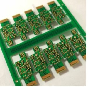
Although carbon ink PCB production does not require the same level of complexity as advanced HDI or high-frequency PCB manufacturing, process control remains critical for achieving stable product performance.
The carbon ink printing process is one of the most important manufacturing steps. The uniformity, thickness, and consistency of the carbon layer directly influence conductivity and contact reliability.
If the carbon ink coating is uneven, certain areas may experience inconsistent electrical performance. Excessive or insufficient coating thickness may also affect contact sensitivity, electrical resistance, and wear resistance.
Therefore, manufacturers must carefully control:
- Carbon ink formulation
- Printing pressure
- Screen printing parameters
- Coating thickness
- Surface alignment accuracy
After printing, the curing process plays a key role in determining the final quality of the carbon layer.
Proper curing temperature and time ensure that the carbon ink fully bonds with the PCB substrate, improving adhesion strength and preventing peeling or cracking during long-term use.
Carbon Ink Layer Reliability and Electrical Performance
The quality of the carbon ink layer directly determines the reliability of a carbon ink PCB.
A well-manufactured carbon coating provides:
- Stable electrical conductivity
- Excellent abrasion resistance
- Strong adhesion to the substrate
- Long operating lifetime
- Consistent contact performance
During production, manufacturers must also ensure compatibility between the carbon ink layer, copper circuits, solder mask, and substrate materials.
Poor process coordination may result in insulation problems, short circuits, or reduced product durability.
Advanced inspection methods help verify carbon layer thickness, surface quality, electrical resistance, and mechanical strength to ensure consistent performance.
For customers requiring rapid design validation and functional testing, PCB Prototype Services enable efficient evaluation of carbon ink PCB designs before mass production.
Advantages of Carbon Ink PCB Compared with Traditional Conductive Methods
Carbon ink PCB technology offers several advantages for specific electronic applications.
Cost Efficiency
Carbon ink printing reduces material costs compared with some traditional metal contact solutions. It is especially suitable for high-volume consumer electronics requiring economical production.
Excellent Wear Resistance
The carbon layer provides strong resistance against mechanical friction, making it ideal for frequently operated buttons and switches.
Simplified Manufacturing Process
Carbon ink printing integrates easily into PCB manufacturing workflows and can reduce assembly complexity in certain applications.
Reliable Low-Current Performance
For low-voltage and low-current circuits, carbon ink provides stable electrical connections while maintaining long-term reliability.
Applications of Carbon Ink PCB in Electronic Products
Carbon ink PCBs are commonly used in industries requiring durable contact solutions and cost-effective circuit designs.
Typical applications include:
- Consumer electronics
- Home appliances
- Industrial control panels
- Measuring instruments
- Automotive control interfaces
- Smart devices
With the continuous development of electronic products, carbon ink PCB technology continues to provide practical solutions for compact, reliable, and cost-sensitive electronic systems.
Advanced PCB Manufacturing Capability for Carbon Ink Solutions
Producing reliable carbon ink PCBs requires comprehensive manufacturing experience, precise process control, and strict quality management.
From carbon ink selection and screen printing optimization to curing process control and final inspection, every step influences the electrical and mechanical performance of the finished PCB.
For advanced circuit board requirements, professional manufacturers also provide solutions such as Multilayer PCB Manufacturing, high-density PCB fabrication, and customized PCB production services.
By combining modern manufacturing technology with engineering expertise, GOPCBA delivers reliable PCB solutions that support a wide range of electronic applications.
Conclusion
Carbon Ink PCB is a specialized PCB technology that combines stable conductivity, excellent wear resistance, and cost-effective manufacturing advantages.
Through precise carbon ink printing, controlled curing processes, and strict quality inspection, carbon ink PCBs can achieve reliable performance in keypads, switches, control panels, and low-current electronic systems.
GOPCBA provides professional carbon ink PCB and customized circuit board manufacturing solutions, helping global customers develop reliable electronic products with high performance and long-term durability.