RF PCB Lamination Structure Design
As a critical platform for high-frequency signal transmission, the lamination structure of an RF PCB directly determines signal stability, transmission loss, and electromagnetic interference resistance.
Compared with conventional circuit boards, RF PCB lamination structures require more precise planning in terms of material selection, layer arrangement, dielectric thickness control, and impedance management. These factors are essential for meeting strict requirements related to signal integrity and high-frequency performance.
A properly designed PCB Layer Stackup ensures that RF signals travel through controlled transmission paths while minimizing signal reflection, energy loss, and unwanted electromagnetic coupling. The optimization of lamination structures is therefore a key factor in producing reliable high-performance RF circuit boards.
Relationship Between Lamination Structure and RF Performance
During high-frequency signal transmission, RF signals are highly sensitive to dielectric loss, electromagnetic interference, and impedance variations. The lamination structure acts as the foundation for controlling these factors.
The effectiveness of an RF PCB structure depends largely on accurate control of signal paths. Through proper material combinations and layer arrangement, manufacturers can maintain stable impedance values, improve impedance matching, and reduce signal reflection.
A well-designed lamination structure also requires strong interlayer bonding. Any voids, air bubbles, or bonding defects between layers may cause signal scattering and additional transmission loss, resulting in signal distortion or reduced communication performance.
The overall thickness consistency of the lamination structure is another important factor. Uneven dielectric thickness may affect impedance stability, mechanical strength, and thermal performance. Excessive thickness variation can introduce signal delays and create heat dissipation problems during long-term operation.
For advanced communication systems, optimized High Frequency PCB Manufacturing processes help maintain stable electrical characteristics while ensuring reliable mechanical performance.
Material Selection Principles for RF PCB Lamination Structures
Material selection is one of the most important considerations in RF PCB lamination design. Different layers require materials with specific electrical and mechanical properties to achieve low-loss and high-stability performance.
Signal layers typically use dielectric materials with low dielectric constant (Dk) and low dissipation factor (Df). These characteristics reduce energy loss during high-frequency signal transmission and improve overall signal quality.
In RF PCB structures, materials used along the primary signal path must provide excellent electrical consistency. Stable dielectric properties help maintain accurate impedance control and minimize variations caused by frequency changes or environmental conditions.
Support and isolation layers require a balance between mechanical strength and insulation performance. These materials must maintain structural stability during fabrication while preventing unwanted signal coupling between adjacent layers.
Thermal expansion compatibility is also a critical factor. Different PCB materials have different coefficients of thermal expansion (CTE). If adjacent materials have significantly different expansion characteristics, high-temperature lamination processes may create internal stress, resulting in cracking, delamination, or reliability issues.
Professional PCB Material Selection and stackup engineering are essential for achieving consistent RF performance in demanding applications.
Layer Arrangement and Signal Isolation in RF PCB Structures
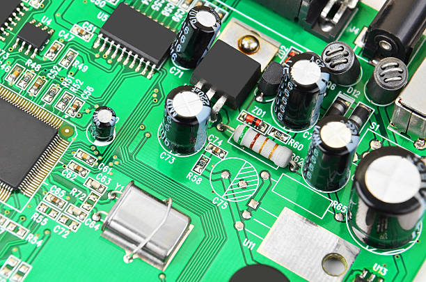
The layer arrangement within an RF PCB lamination structure plays a vital role in signal isolation and electromagnetic control.
By carefully positioning signal layers, ground planes, and power layers, engineers can create effective shielding structures that reduce electromagnetic interference and improve signal integrity.
For example, placing a continuous ground plane beneath a high-frequency signal layer provides a controlled return path and helps absorb unwanted electromagnetic radiation. This configuration reduces coupling between adjacent signal layers and improves transmission stability.
The spacing between different functional layers must also be precisely controlled. The required distance depends on signal frequency, operating power, dielectric properties, and impedance requirements.
If the distance between layers is too small, excessive parasitic capacitance may occur, affecting signal speed and waveform quality. If the spacing is too large, the PCB structure may become less stable and signal transmission paths may become more sensitive to external interference.
For multilayer RF PCB designs, optimized layer positioning allows multiple high-frequency signals to operate independently within limited board space while maintaining excellent electrical performance.
Thickness Control and Impedance Management
Thickness control is a fundamental requirement in RF PCB lamination structure design.
The dielectric thickness between copper layers directly affects characteristic impedance. Even small variations in dielectric thickness can influence impedance values, resulting in signal reflection and transmission loss.
Therefore, manufacturers must precisely control:
- Dielectric material thickness
- Copper foil thickness
- Lamination pressure
- Resin flow characteristics
- Layer registration accuracy
These factors work together to determine the final electrical performance of the RF PCB.
Advanced Multilayer PCB Manufacturing technologies enable accurate stackup control and reliable production of complex RF circuit boards with multiple signal layers and controlled impedance requirements.
Manufacturing Challenges of RF PCB Lamination Structures
Producing reliable RF PCB lamination structures requires advanced manufacturing capabilities and strict process control.
High-frequency materials are often more sensitive than standard FR-4 materials, requiring careful handling during drilling, lamination, and surface processing.
Common manufacturing challenges include:
- Maintaining precise layer alignment
- Controlling dielectric thickness variation
- Preventing delamination
- Reducing material deformation
- Maintaining consistent electrical properties
To overcome these challenges, manufacturers must combine advanced equipment, experienced engineering teams, and comprehensive quality inspection systems.
Prototype verification is also important for RF applications. Through PCB Prototype Services, engineers can validate stackup designs, evaluate signal performance, and optimize manufacturing parameters before full-scale production.
Importance of RF PCB Lamination Structure Optimization
The lamination structure of an RF PCB is a critical factor influencing high-frequency performance. Every design detail, from material selection and layer arrangement to thickness control and bonding quality, affects signal transmission accuracy.
A properly optimized RF PCB structure provides:
- Stable impedance control
- Lower signal transmission loss
- Improved electromagnetic compatibility
- Better thermal reliability
- Enhanced long-term performance
As electronic systems continue to demand higher frequencies and faster data transmission rates, advanced RF PCB lamination technology becomes increasingly important.
Conclusion
The RF PCB lamination structure is the foundation of reliable high-frequency signal transmission. Through optimized material selection, precise layer stackup design, and strict manufacturing control, PCB manufacturers can achieve excellent signal integrity and long-term reliability.
GOPCBA provides professional RF PCB manufacturing solutions, combining advanced fabrication technology and engineering expertise to support high-frequency communication, wireless systems, automotive electronics, and other demanding applications.
By continuously improving lamination processes and material management, GOPCBA helps customers develop high-performance RF circuit boards that meet the requirements of modern electronic technologies.