PCB Etch Back Process and Its Importance in PCB Manufacturing
Among the many processes involved in PCB Manufacturing, PCB Etch Back is a critical technology that has a significant impact on circuit board performance, reliability, and long-term stability.
Unlike simple copper removal processes, etch back is a precisely controlled surface treatment technology that modifies the copper layer structure to improve interlayer bonding, electrical connection reliability, and high-frequency signal performance.
For advanced PCB products such as Multilayer PCB, high-frequency circuit boards, and HDI PCB, the accuracy of the etch back process directly affects whether the final product can meet demanding application requirements.
By optimizing copper surface characteristics and improving layer-to-layer integration, PCB etch back technology provides a reliable foundation for high-performance electronic systems.
Core Value and Function of PCB Etch Back
The primary purpose of PCB Etch Back is to selectively remove a controlled amount of copper material from the PCB surface to create an optimized microscopic structure.
This process is not designed to simply reduce copper thickness. Instead, it adjusts the copper surface morphology to enhance adhesion between copper layers and dielectric materials while improving electrical performance.
During the lamination process, copper surfaces treated through etch back achieve stronger bonding with substrate materials. This improved interface strength helps prevent common reliability problems such as:
- Layer separation
- Delamination
- Internal voids
- Poor interlayer connection
For complex multilayer circuit structures, strong interlayer bonding is essential. A precisely controlled etch back process improves structural stability and ensures reliable operation under thermal cycling, mechanical stress, and long-term usage conditions.
In addition, proper etch back treatment can reduce copper surface defects and irregularities, minimizing signal interference during transmission. This is especially important for High Frequency PCB applications where signal integrity is highly sensitive to conductor surface conditions.
PCB Etch Back Requirements for Different PCB Applications
Different PCB structures have different performance requirements, meaning that etch back parameters must be adjusted according to board design, material characteristics, and application environment.
Etch Back Requirements for Multilayer PCB
Advanced Multilayer PCB structures often contain numerous conductive layers with complex electrical and thermal distributions.
The etch back process must improve interlayer adhesion while avoiding excessive copper removal that could reduce conductor thickness and affect current-carrying capability.
Precise control of:
- Etch depth
- Surface roughness
- Chemical concentration
- Processing time
is necessary to ensure that each copper layer maintains reliable electrical performance while achieving strong bonding with adjacent dielectric materials.
A properly optimized process improves multilayer structural stability and reduces potential failures caused by thermal stress or mechanical deformation.
Etch Back Control for High Frequency PCB Performance
High-frequency circuit boards require extremely stable signal transmission characteristics.
For High Frequency PCB manufacturing, copper surface conditions directly influence signal loss, reflection, and transmission efficiency.
If the copper surface becomes excessively rough, high-frequency signals may experience increased conductor loss and signal distortion due to the skin effect.
Therefore, etch back processing must achieve a balance between:
- Improved bonding strength
- Controlled surface roughness
- Stable electrical performance
Improper etch back treatment may introduce microscopic defects that interfere with signal transmission paths.
Through precise process management, manufacturers can reduce unwanted signal loss and maintain better signal integrity for RF communication, networking equipment, and high-speed electronic systems.
Etch Back Challenges in HDI PCB Manufacturing
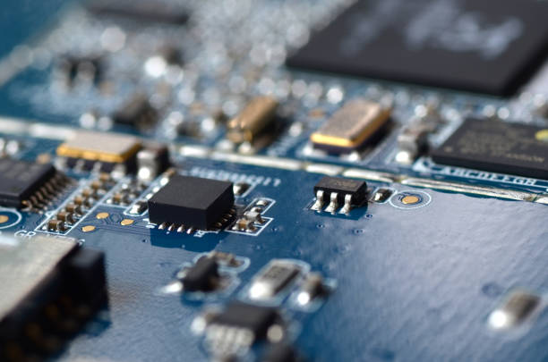
HDI PCB technology is characterized by high-density routing, fine line structures, and advanced interconnection methods.
Because HDI boards require extremely high circuit accuracy, etch back precision directly affects line definition, insulation performance, and manufacturing yield.
If etch back is insufficient:
- Copper residues may remain on circuit edges
- Surface defects may increase
- Short circuit risks may rise
If etch back is excessive:
- Circuit width may become reduced
- Electrical resistance may increase
- Fine-line reliability may decrease
Therefore, HDI PCB production requires highly controlled etch back processes to achieve precise copper surface treatment while maintaining fine circuit dimensions.
For advanced designs, professional HDI PCB Manufacturing capabilities ensure accurate process control and reliable high-density interconnections.
Manufacturing Control and Quality Management of PCB Etch Back
The success of PCB etch back depends on precise control throughout the manufacturing process.
Key control factors include:
- Chemical solution composition
- Processing temperature
- Etching speed
- Treatment duration
- Copper surface inspection
Manufacturers must continuously monitor process conditions to maintain consistent results across different PCB materials and structures.
Advanced inspection methods help evaluate:
- Surface morphology
- Copper thickness variation
- Bonding quality
- Electrical performance
For customers developing new electronic products, PCB Prototype Services allow early validation of etch back parameters and PCB performance before full-scale production.
Importance of PCB Etch Back in Advanced Circuit Board Manufacturing
As electronic devices continue to become smaller, faster, and more powerful, PCB manufacturing requires increasingly precise surface treatment technologies.
PCB etch back plays an essential role in improving:
- Interlayer bonding strength
- Signal transmission reliability
- Thermal durability
- Structural stability
- Manufacturing consistency
Combined with advanced PCB Manufacturing Services, optimized etch back technology enables manufacturers to produce reliable circuit boards for demanding industries.
Applications include:
- Telecommunications equipment
- Automotive electronics
- Industrial control systems
- Medical devices
- High-speed computing platforms
Conclusion
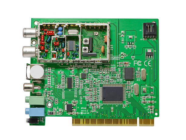
PCB Etch Back is a key technology that supports the reliability and performance of modern high-end circuit boards.
Through precise control of copper surface treatment, manufacturers can improve interlayer adhesion, enhance signal integrity, and increase the durability of multilayer PCB structures.
For advanced applications requiring high density, high frequency, and high reliability, professional process control is essential.
GOPCBA applies advanced PCB manufacturing technologies and strict quality management systems to provide reliable circuit board solutions for global customers, supporting the development of next-generation electronic products.