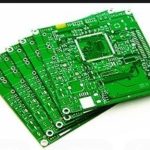
Wearable Payment PCB Guide: Materials, Cost and Process
Tap-to-pay has changed the way the world buys coffee, rides transit, and enters buildings. Smartwatches, fitness bands, payment wristbands, and smart rings now carry the payment credentials that used to live in a physical card. Inside each of these devices, a small printed circuit board makes contactless payment possible. The wearable payment PCB integrates the NFC chip, antenna, microcontroller, and power circuitry into a package slim enough to wear every day and robust enough to survive daily life. For fintech companies, wearable brands, and electronics manufacturers, understanding the materials, processes, and costs behind this board is essential. This guide explains the complete picture, from material selection to volume pricing in 2025.
What Is a Wearable Payment PCB?
A wearable payment PCB is a miniaturized, frequently flexible circuit board that enables secure payment functions inside wearable devices. It connects the NFC controller, security element, antenna, and supporting components so the device can communicate with payment terminals through near-field communication. The board also manages power from a small battery and links to the device’s main processor for transaction status and user feedback.
Common applications include smartwatches with contactless payment, fitness bands with embedded payment chips, smart rings used for retail and transit, and payment wristbands issued at events or theme parks. Each form factor imposes different constraints: a ring needs extreme miniaturization, a watch has more room but demands long battery life, and a wristband must flex continuously with the wearer’s movement.
What unites them is the requirement for security. Payment data is sensitive, so the PCB layout must protect the encryption module from probing and interference. A well-designed wearable payment board delivers the same level of trust as a bank card, but inside a device that bends, sweats, and gets knocked against door frames all day.
Key Materials for Wearable Payment PCBs
Material selection determines performance, durability, and cost more than any other decision in a wearable payment board project.
FR-4 substrate is used for rigid sections that carry the main processor and connectors. It offers high strength and dimensional stability, which protects delicate ball grid array packages from mechanical stress.
Flexible substrates such as polyimide (PI) and PET allow the circuit to bend around curved watch cases or fold inside a ring housing. Polyimide is the premium choice because it withstands repeated flexing and soldering temperatures; PET suits simpler, lower-cost constructions.
Copper foil provides the conductive traces and the NFC antenna loops. Thinner, rolled-annealed copper flexes better than standard electrodeposited foil, so antenna and flex-circuit designers often specify it for dynamic bending zones.
Silver paste and conductive polymers appear in advanced thin flexible boards where printing conductive traces directly onto film reduces thickness and weight.
Protective coatings such as solder mask and conformal coating guard against moisture, sweat, and abrasion. In wearable payment products, a thin conformal coating over the assembled module is common because users wear the device while washing hands or running in the rain.

Manufacturing Process for Wearable Payment PCBs
Producing a wearable payment board follows a sequence of precision steps. It starts with high-density design in CAD software, where the engineer places the NFC chip, security element, and antenna within a very tight outline. Next, multilayer stack-up and lamination press the flexible and rigid layers together; rigid-flex boards alternate stiff islands with flexible bridges in a single lamination cycle.
Laser drilling creates the microvias that connect layers in dense areas, and copper plating forms reliable conductive walls. Circuit patterning by etching produces the fine lines and the precise antenna geometry that NFC performance depends on. Surface finish selection follows, with ENIG common on fine-pitch pads and immersion silver or OSP used where cost matters.
Surface-mount technology then places the components. Tiny NFC controllers, crystals, and passives require accurate solder paste printing and placement. After reflow, the boards move through testing: functional checks verify NFC communication range and transaction behavior, impedance tests confirm antenna tuning, and durability tests subject samples to bending cycles. For fintech certification, the assembled module may also need additional security evaluation, so the manufacturing flow must support strict traceability. Reviewing the test coverage available through PCBA testing early in the project prevents certification surprises later.

Cost Factors and Price Ranges
The price of a wearable payment PCB is shaped by materials, design complexity, volume, and customization. Flexible polyimide substrates cost more than standard FR-4, and rigid-flex construction adds lamination and processing steps. High-density miniaturized circuits require finer tooling and tighter process control. Small prototype batches carry much higher unit prices than volume production. Special coatings and security-related design rules add further cost.
Realistic 2025 price bands help with budgeting. Simple single-layer boards in high volume range from $2 to $5 per board. Flexible and rigid-flex boards run $8 to $20 per board depending on layer count and antenna design. High-density multilayer boards in small series range from $25 to $50 per board. Fully assembled payment modules, including the NFC controller and security element, sit higher because the bill of materials dominates the total.
Manufacturing Challenges and Solutions
Wearable payment boards push manufacturing technology to its limits in four areas.
Miniaturization. Fitting a secure payment system inside a ring or a slim band requires high-density interconnect layout, microvias, and chip-scale packages. The solution is design experience: every trace earns its place, and unnecessary features are removed before the layout is finalized.
Thermal management. Small enclosures trap heat during charging and intensive use. Thermal vias, copper pours, and careful placement of hot components keep temperatures within safe limits without adding thickness.
Flex durability. A payment band may flex tens of thousands of times. Dynamic flex zones need tear-resistant copper, controlled bend radii, and strain relief at every transition from rigid to flexible material.
Security integration. Payment encryption modules must be protected against physical attack. Layout rules keep sensitive traces internal, ground shields surround the security element, and the board avoids exposed test points near the encryption section. These rules are part of the design specification, not an afterthought.
Addressing these challenges during the design-for-manufacturability review, ideally with the fabrication partner, is the fastest route to a reliable product. A factory that understands flex circuits and high-density assembly can flag risks before tools are cut. You can assess whether a supplier fits your program by reviewing its PCB capabilities and quality management system before committing a design.
Global Market Price Insights
Manufacturing location creates clear price differences for wearable payment PCBs. Chinese factories produce high-volume boards at $5 to $15 per board, offering the strongest combination of cost, capability, and speed. US suppliers typically quote $15 to $35 per board because of labor and overhead, while European manufacturers range from $20 to $40 per board with stricter compliance documentation.
Flexible PCB production costs slightly more everywhere, but its role in wearable payment products is irreplaceable, so demand keeps rising. Global buyers increasingly source from Asia for volume products while keeping prototype and early-stage work close to their engineering teams. The winning structure for many fintech hardware startups is to validate locally, then transfer the proven design to an Asian volume partner for cost-efficient scale.
NFC Antenna Design on the Payment Board
The NFC antenna deserves special attention because it determines whether the payment actually works. The antenna is typically printed on the PCB itself, with its loop size, trace width, and number of turns tuned to a specific inductance and resonant frequency. The surrounding metal, battery, and case materials all shift the tuning, so the antenna must be co-designed with the mechanical enclosure.
Ferrite sheets are often laminated behind the antenna to shield it from the battery and metal chassis, improving read range. After assembly, every unit should pass a communication test that verifies it can exchange data with a reference reader at the required distance. Paying attention to antenna consistency during PCB production, rather than fixing it in firmware, keeps transaction success rates high in the field.
Why Choose a Specialized Manufacturer
Not every PCB factory can produce wearable payment boards well. Look for a partner with real rigid-flex experience, fine-pitch SMT capability, and NFC testing competence. Ask about antenna tuning support, conformal coating options, and whether the factory has produced boards for fintech or payment clients before. Prototype turnaround of five to seven days and production lead times of two to three weeks are reasonable expectations from an efficient supplier.
A specialized manufacturer also helps with the cost-quality balance. Volume pricing for flexible payment boards can start around $6 per board, and free DFM feedback during quoting removes design waste before money is spent. When fabrication and PCB assembly live in the same organization, the payment module arrives tested and ready rather than as a bare board that must be handed to a second vendor.
Component supply is another factor that separates smooth wearable programs from delayed ones. NFC controllers, security elements, and ultra-thin batteries have long lead times and are sometimes allocated, so the factory should help plan procurement before the design is finalized. Factories that offer components-procurement support can secure the payment silicon early, stage it for scheduled production, and avoid last-minute substitutions that would require re-qualification of the security module.
Future Trends in Wearable Payment PCBs
Several trends will shape the next generation of wearable payment boards. Ultra-thin and bendable circuits will keep improving wearing comfort, pushing materials like LCP into mainstream designs. Eco-friendly substrates and lead-free processes will expand in response to sustainability requirements from both regulators and consumers. IoT and AI integration will let payment wearables combine transactions with health data and smart assistants, adding processing power to the same tiny board. Higher energy efficiency will extend battery life, which matters because a payment device that dies mid-transaction is worse than useless.
As the industry evolves, the fundamentals stay the same: secure layout, reliable flex construction, and disciplined testing. Brands that master those fundamentals, with the right manufacturing partner behind them, will lead the contactless payment market.
Frequently Asked Questions
Q1. How much does a wearable payment PCB cost? Prices typically range from $5 to $50 per board depending on material, design complexity, and volume.
Q2. How long does production take? Prototypes usually take five to seven days, and volume production about two to three weeks.
Q3. Are flexible PCBs better for wearable payment devices? Yes, flexible and rigid-flex boards fit curved enclosures better, improve comfort, and save internal space.
Q4. Can manufacturers provide customized services? Yes, qualified partners offer custom design, production, and assembly tailored to each wearable payment product.
Q5. How is payment security handled on the board? The encryption module is isolated with internal routing and shielding, and the design follows fintech security guidelines for tamper resistance.
Q6. What is the minimum order quantity for prototypes? Most qualified suppliers accept prototype orders from five to ten boards, which is enough for certification testing and field trials.
Q7. Can the NFC antenna be printed directly on the flexible PCB? Yes, printing the antenna loop directly on the flex layer is the standard approach for compact wearables, with ferrite shielding added to protect against nearby metal and batteries.
Conclusion
The wearable payment PCB is the quiet enabler of modern contactless payment. Its design and manufacture must balance security, flexibility, and durability inside a space measured in millimeters. Material choice, process discipline, and production volume all influence price, and a capable manufacturing partner brings those variables into balance. With the right approach, fintech brands can deliver payment wearables that are secure, comfortable, and affordable, ready for the tap-to-pay future.