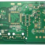
RAM PCB Guide: Structure, Design and Manufacturing Basics
Memory is the fastest-moving part of any computer, and the circuit board that carries it has to keep pace. A RAM PCB is far more than a strip of fiberglass with chips on it: the board itself is an electrical transmission system that decides how cleanly data moves between the processor and the memory chips. For engineers, buyers, and anyone who has watched a computer mysteriously crash under load, understanding RAM circuit board structure, design, and manufacturing is valuable knowledge. This guide explains what a RAM PCB is, how it is built, the design challenges of high-speed signals, the production steps, realistic costs, and what to look for in a manufacturer.
What Is a RAM PCB?
A RAM PCB, often called a memory module board, is the printed circuit board that carries DRAM or SDRAM chips and connects them to the computer motherboard. The board provides the mechanical support and the precise electrical pathways that let the memory chips communicate with the processor at billions of transfers per second. In desktop and laptop systems the board is a long, narrow module with gold edge contacts, while in embedded products the memory chips may sit on the main system board itself.
Because memory signals are extremely fast and sensitive, a RAM circuit board is engineered like a small microwave system. Trace length, impedance, spacing, and layer stackup all affect whether data arrives intact. A board with excellent chips but poor layout will produce errors, instability, or reduced overclocking headroom, which is why serious memory products are designed and tested with the same care as the chips they carry.
Structure and Layers of a RAM Circuit Board
The internal structure of a RAM module determines how well it performs. Memory chips are soldered onto the surface and connect through the board to the gold finger edge connector. Copper traces form the data, address, and control highways between the chips and the connector. Dedicated power and ground layers distribute voltage evenly and give signals a clean return path, which suppresses noise. Dielectric layers between the copper planes use materials such as FR-4 or, for higher grades, low-loss laminates that preserve signal quality. Modern modules are almost always multilayer designs: typical DDR4 modules use six to eight layers, and high-performance or server modules can exceed ten layers to isolate the many parallel signals from each other and from power noise.
How RAM PCBs Function in a System
When the processor needs data, the memory controller sends address and command signals through the module connector, and the RAM chips respond by driving data back over the same bus. What makes this remarkable is the speed: a single data transfer happens in fractions of a nanosecond, and the board must deliver every bit with controlled timing. The board does this through carefully matched trace lengths, which keep the many parallel signals arriving together, and controlled impedance, which prevents reflections when a signal reaches the end of a trace. Power integrity matters just as much, because the memory chips switch millions of times per second and need stable voltage right at the pins. Thermal behavior is the final piece: hot memory errors appear first, so quality boards carry heat away from the chips through the laminate and into the airflow.
Types of Memory PCBs
Memory boards come in different grades for different markets. Entry-level modules use simpler stackups and standard materials, keeping cost low for everyday desktops and laptops. High-density modules add more layers and finer routing, and they are used in servers, gaming systems, and workstations that demand maximum bandwidth and reliability. Small outline modules shrink the physical format for laptops and small-form-factor computers. In smartphones, tablets, and IoT products, memory is often packaged directly onto the main board in a compact layout rather than on a separate module. The choice of type is a balance of speed, capacity, physical space, and budget, and each design requires its own stackup and routing rules.

RAM PCB Manufacturing Process
Producing a memory module involves a sequence of precise operations. Design and layout come first, with routing optimized for equal-length, impedance-controlled traces, which is where skilled PCB design and layout work makes the biggest difference. Material selection follows, with high-speed boards using controlled dielectric laminates. The inner layers are patterned and laminated into a precise stackup, keeping every layer aligned. Copper is etched to form fine traces, and drilling and plating create the vias that connect layers. The edge connector area receives the gold plating that survives thousands of insertions. Memory chips are then assembled with careful soldering, and each module is tested with electrical tests, thermal analysis, and functional validation at speed. Because a single bad trace can corrupt data intermittently, reputable manufacturers test every module, not just a sample, before shipment.
Applications of RAM Circuit Boards
Memory PCBs support virtually every computing device. Desktop and laptop computers are the most familiar use, where stability under heavy multitasking is essential. Smartphones and tablets require compact, high-density boards that fit tiny enclosures. Servers and data centers rely on high-speed modules that keep thousands of processors fed with data around the clock. Gaming computers and workstations need boards that tolerate overclocking and sustained high loads. Embedded and IoT systems use small, low-power memory configurations integrated into control boards. In each environment the design priorities shift, but the fundamentals of clean power, matched timing, and thermal control remain the same.
Design Challenges in Memory PCB Design
High-speed memory design is demanding because the margin for error is measured in picoseconds. Signal integrity is the biggest challenge: crosstalk between tightly spaced traces, impedance mismatches at connectors, and noise from power planes all corrupt data at speed. Designers counter these effects with controlled impedance stackups, ground plane isolation between signal groups, and careful trace spacing. Miniaturization adds pressure because smaller devices force traces closer together while speeds keep rising. Thermal management is difficult in thin laptops where airflow is scarce, so designers use copper pours and optimized component placement to spread heat. Finally, cost versus performance is an ever-present trade-off: premium laminates and more layers improve signals but raise price, so the design must hit the performance target without overbuilding.
Memory Module Standards and Formats
Compatibility with the host system is defined by a mix of electrical and mechanical standards, and the board layout must honor both. Full-size DIMMs serve desktops and servers, while the shorter SO-DIMM format fits laptops and small-form-factor machines. Registered and load-reduced modules used in servers add buffering chips that change the electrical loading, so their boards carry extra components and follow stricter routing rules. Each memory generation, from DDR4 to DDR5 and LPDDR5, specifies different voltages, pin counts, key notches, and signal groups, which means the PCB layout, stackup, and edge connector design all change between generations. Buyers should therefore order boards that match the exact module standard and platform requirement, because a board built to the wrong generation cannot be adapted with firmware.
Future Trends in RAM PCB Technology
Memory technology keeps pushing the board forward. DDR5 and LPDDR5 modules run at higher speeds with tighter timing margins, requiring even better-controlled stackups. Advanced base materials such as low-loss glass-reinforced laminates are appearing in premium products. AI-assisted layout tools help engineers solve complex routing problems faster. Miniaturization continues for wearables and IoT, while server modules grow in layer count and routing density to support the next generation of processors. Manufacturers that invest in fine-line capability, precise lamination, and high-speed testing will be the ones able to serve these demanding products.
RAM PCB Cost
The price of a RAM PCB depends on size, layer count, material grade, and gold finger finish. Standard modules typically cost in the range of 1.50 to 5 dollars per bare board for ordinary FR-4 constructions at moderate volume. High-density boards with eight or more layers, low-loss materials, and strict impedance control cost more, and server-grade modules with extensive testing sit at the top of the range. Assembly of the memory chips, functional testing, and packaging add further cost. Buyers should compare quotes that include the full specification because a cheap board with uncontrolled impedance will fail at speed and cost far more in returns and lost trust than the money saved on the initial purchase.
How to Choose a RAM PCB Manufacturer
Choosing the right producer matters more for memory than for many other boards. Look for a factory with experience in high-speed multilayer design, because impedance control is learned through process discipline, not promised in a brochure. Confirm its layer capability, minimum trace and spacing, and whether it can hold the tight tolerances that memory routing requires. Ask about material suppliers and whether controlled dielectric laminates are available. Verify testing practice: electrical test, impedance verification, and thermal cycling are the checks that catch defective modules before they reach users. Check certifications such as ISO and IPC compliance, and look for transparent communication on lead times, which typically run about 7 to 12 working days for standard orders with faster service available. A partner that can move from PCB manufacturing through assembly and PCBA testing in one place simplifies the project and keeps quality control in a single chain.

Design for Manufacturing and Testing
Memory boards are demanding to build, so the design should be reviewed for manufacturability before tooling starts. Layer registration tolerances, minimum trace widths, via sizes, and the balance of the stackup all need to fit the factory capability, and impedance coupons on the panel let the manufacturer verify that the controlled impedance actually matches the target. Thermal reliefs on power planes, test points on every critical net, and clean breakout patterns under fine-pitch memory chips make assembly and testing reliable. Gold finger edges need precise plating thickness and a chamfer so the module inserts cleanly. Once built, every module should pass functional testing at its rated speed and temperature, because marginal timing shows up only under load. A partner with documented PCB capabilities and full PCB assembly in-house can validate the design, build the boards, and test the finished modules under one roof, which shortens the loop when a change is needed.
Frequently Asked Questions
Q1. How much does a RAM PCB cost? Standard modules typically cost about 1.50 to 5 dollars per board, while high-density or server-grade boards with more layers and premium materials cost more.
Q2. How long does RAM PCB production take? A typical order takes 7 to 12 working days, with expedited service available when a project is behind schedule.
Q3. Can RAM PCBs be customized? Yes, buyers can specify layer count, thickness, trace width, materials, gold finger finish, and test standards to match a specific application.
Q4. Why is my computer unstable with certain memory modules? Instability is often caused by uncontrolled impedance, inadequate power delivery, or poor thermal design on the module, which is why quality manufacturing and testing matter.
Q5. Are more layers always better for RAM PCBs? More layers improve signal isolation and power delivery but add cost; the right count depends on the memory standard, speed grade, and module format.
Conclusion
A RAM PCB is the unsung carrier of computing performance. From the layer stackup to the last millimeter of copper routing, every detail influences how fast and how reliably a system runs. Understanding the structure, design constraints, manufacturing steps, and cost drivers helps engineers and buyers choose memory boards that deliver clean signals under real workloads. With disciplined design, quality fabrication, and thorough testing, a RAM circuit board quietly does its job for years, letting the processor focus on what it does best.