PCB Quality Standards: PCB Visual Inspection & IPC Class 2 Criteria
When a PCB is received and an apparent appearance defect is found during visual inspection, the board should not be immediately rejected or scrapped. The first step is to evaluate the condition according to the applicable IPC requirements, customer specifications, engineering drawings, and agreed acceptance criteria.
Unless otherwise specified by the customer, IPC Class 2 is commonly used as a baseline acceptance level for general electronic products. The following inspection criteria provide a practical reference for evaluating PCB appearance and manufacturing quality.
Dimensional accuracy is one of the first items to verify during PCB Visual Inspection. PCB length, width, board thickness, routing features, and V-CUT dimensions should be checked against the manufacturing drawing and specified tolerances.
Unless special dimensional requirements are specified, a typical manufacturing control value for PCB length and width is:
PCB length and width tolerance: ±0.15 mm
For precision applications, however, the actual tolerance should always be determined according to the PCB drawing and customer requirements.
For boards manufactured with V-CUT scoring, the remaining thickness should be controlled consistently to ensure reliable depanelization without damaging the PCB.
As a general manufacturing reference:
Actual V-CUT requirements may vary depending on board thickness, material, panel design, and depanelization method.
Bow and twist can affect component placement, soldering, assembly stability, and automated production. Therefore, board flatness is an important part of PCB Quality Control.
For PCBs used with surface-mount components, the maximum allowable bow and twist is commonly controlled at:
0.75%
For other types of printed circuit boards, the commonly referenced maximum value is:
1.5%
The applicable IPC specification and customer requirements should be used for the final acceptance decision.
Bow = H / L × 100%
Where:
The calculated percentage represents the amount of board curvature relative to its length or width.
Twist = S / D × 100%
Where:
The twist measurement should be evaluated across the full diagonal of the PCB.
Solder mask coverage should be checked around pads, vias, holes, and other exposed copper areas.
For solder mask covering requirements, the height of cured solder mask above the associated copper pad should remain within the applicable IPC acceptance criteria. A commonly referenced limit is that the solder mask should not extend more than approximately 50 μm above the copper surface where the applicable specification requires this condition.
During inspection, particular attention should be paid to:
The final acceptance decision should be based on the applicable IPC class and customer specification.
Haloing refers to localized separation or whitening around holes or mechanical features caused by stress or damage to the laminate.
Minor haloing does not necessarily mean that the PCB must be rejected. The key factors are its size, location, severity, and whether it affects the electrical, mechanical, or structural integrity of the board.
During PCB Visual Inspection, inspectors should determine whether haloing:
Exposed glass fabric occurs when the resin does not completely cover the underlying fiberglass reinforcement.
A small amount of visible fabric does not automatically indicate a defective PCB. However, the condition should be evaluated according to its location, extent, severity, and effect on board performance.
Special attention should be given to exposed fabric located near:
The acceptance decision should follow the applicable IPC requirements rather than relying solely on visual appearance.
Surface voids are localized cavities or imperfections that may appear within the PCB surface or laminate structure.
Not every visible void represents a functional defect. The evaluation should consider the void’s size, quantity, location, depth, and potential influence on electrical insulation, mechanical strength, or long-term reliability.
A proper PCB Quality Standards inspection should distinguish between cosmetic imperfections and defects that can affect product performance.
Delamination refers to separation between layers or between the laminate and copper structure. Blistering is another form of localized separation that can appear as a raised area on the PCB surface.
Possible causes include:
Delamination and blistering should be treated more seriously than purely cosmetic defects because they may affect the structural integrity and long-term reliability of the PCB.
Boards showing significant delamination or blistering should be evaluated against the applicable IPC acceptance criteria and customer requirements before being accepted.
Plating voids are areas where copper plating is incomplete or absent, particularly inside plated-through holes or on conductive surfaces.
Because plated holes provide electrical connections between PCB layers, plating integrity is critical to board functionality.
During inspection, check for:
Plating defects that compromise electrical connectivity or reliability should not be treated as simple cosmetic imperfections.
PCB silkscreen should be clear, legible, correctly positioned, and consistent with the approved manufacturing data.
Inspectors should check for: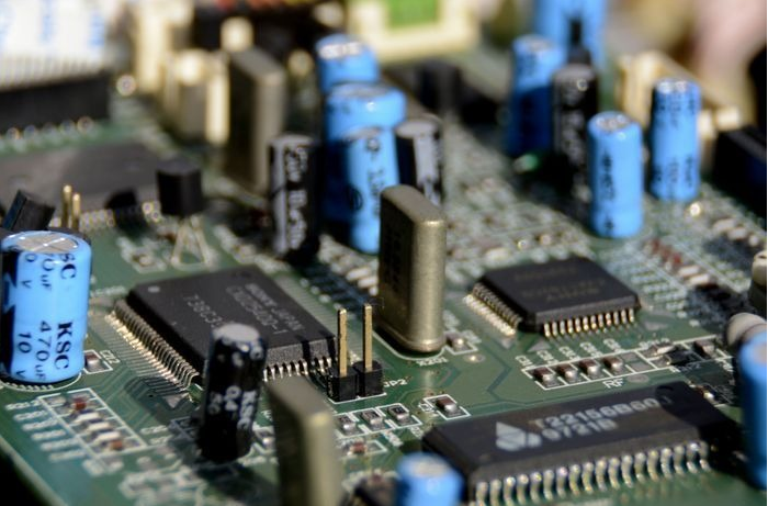
Silkscreen should not interfere with soldering areas, electrical contacts, or component placement.
For production projects, proper design review before fabrication can help prevent many silkscreen and manufacturability problems. GOPCBA provides PCB Design & Layout support as part of its electronics manufacturing services.
Trace width is a critical parameter affecting current-carrying capability, electrical performance, impedance, and manufacturing yield.
During inspection, the measured conductor width should be compared with the approved PCB design data and manufacturing tolerances.
The evaluation should consider:
For high-speed or high-current designs, conductor width should not be evaluated independently from copper thickness, impedance requirements, and the overall stack-up.
Conductor spacing is the distance between adjacent traces, pads, copper areas, or other conductive features.
Insufficient spacing may increase the risk of:
The minimum spacing should therefore be checked against the PCB design rules, voltage requirements, manufacturing capabilities, and applicable IPC criteria.
A professional PCB manufacturer should verify spacing during both design review and manufacturing inspection.
PCB appearance inspection should not be considered an isolated final step. PCB quality needs to be controlled throughout design, material preparation, fabrication, inspection, and testing.
A reliable PCB Manufacturing process should include controls covering:
GOPCBA’s manufacturing process incorporates process monitoring, final inspection, and electrical testing to verify PCB quality before shipment.
For projects that proceed directly from PCB fabrication to assembly, early inspection is especially important because PCB defects can later affect solder paste printing, component placement, soldering, inspection, and overall PCBA yield.
A PCB that passes dimensional and appearance inspection provides a stronger foundation for subsequent assembly.
During SMT and through-hole production, PCB flatness, pad condition, solder mask quality, surface finish, and dimensional accuracy can directly influence assembly performance.
GOPCBA’s PCB assembly process includes incoming material inspection, BOM verification, process control, AOI, X-ray inspection, ICT, functional testing, and final inspection according to project requirements.
For prototype projects, early PCB inspection is also important because identifying manufacturing issues before larger production runs can reduce rework and production risk. GOPCBA supports prototype PCB assembly from design review and PCB manufacturing through assembly and testing.
Even when a PCB passes final inspection, improper storage can negatively affect its quality before assembly.
PCBs should therefore be stored and handled under appropriate environmental conditions. General good practices include:
Storage requirements may vary according to PCB material, surface finish, packaging method, and intended assembly process. Customer specifications and material manufacturer’s recommendations should take priority.
A visible imperfection does not automatically mean that a PCB is unusable.
The correct evaluation process should be:
Visual Observation → Measurement → IPC/Customer Specification Review → Functional Risk Assessment → Final Acceptance Decision
This approach prevents unnecessary scrap and helps distinguish between acceptable cosmetic variations and defects that can affect PCB performance or reliability.
A PCB should be considered for rejection or rework when the defect:

Reliable PCB production requires more than a final visual inspection. Quality must be controlled from engineering review through fabrication, assembly, testing, and shipment.
GOPCBA applies a structured quality management approach covering PCB design review, DFM, PCB manufacturing, component procurement, PCBA manufacturing, testing, and final inspection. Its quality system references ISO 9001, IPC-A-610E, and SPC-based process control.
For customers requiring a complete electronics manufacturing workflow, GOPCBA integrates PCB fabrication, component sourcing, SMT/THT assembly, inspection, testing, and other manufacturing services within a one-stop production model.
For additional information about manufacturing quality and inspection capabilities, visit GOPCBA’s Quality Management service page.
PCB appearance quality should always be evaluated using objective measurements and applicable industry standards rather than visual judgment alone.
Key inspection items include PCB dimensions, V-CUT accuracy, bow and twist, solder mask coverage, haloing, exposed glass fabric, surface voids, delamination, plating voids, silkscreen quality, conductor width, and conductor spacing.
By combining PCB Quality Standards, controlled manufacturing processes, professional inspection, and electrical testing, manufacturers can reduce unnecessary rejection, improve production consistency, and increase PCB reliability.
For projects ranging from prototypes to volume production, a qualified manufacturing partner should be able to control PCB fabrication and assembly quality throughout the entire production process.