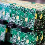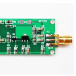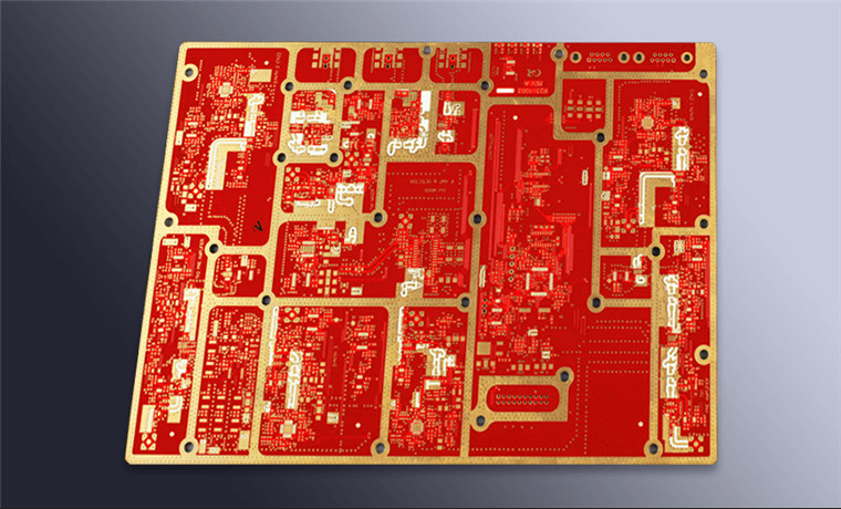
A PCB Circuit Board, or Printed Circuit Board (PCB), is one of the fundamental components used in modern electronic products. It provides mechanical support for electronic components while creating electrical connections between components through conductive copper patterns.
From simple consumer electronics to industrial control systems, automotive electronics, communications equipment, medical devices, and high-performance computing systems, PCBs are essential to modern electronic hardware.
Understanding PCB Materials, board structures, and the manufacturing process is important for engineers, product developers, purchasers, and anyone involved in electronic manufacturing.
1. What Is a PCB Circuit Board?
PCB stands for Printed Circuit Board. It is also commonly referred to as a printed wiring board (PWB).
A PCB is an insulating substrate containing precisely designed conductive patterns. These patterns connect electronic components and provide the electrical interconnections required by the circuit.
A typical PCB may contain:
- Copper traces.
- Solder pads.
- Via holes.
- Plated through-holes.
- Power and ground planes.
- Component footprints.
- Solder mask.
- Silkscreen markings.
- Mechanical mounting features.
The basic functions of a PCB Circuit Board are to provide:
- Electrical interconnection between components.
- Mechanical support for electronic components.
- Signal and power distribution throughout the circuit.
- Thermal and structural support where required.
Unlike traditional point-to-point wiring, PCB technology integrates electrical connections into a compact and repeatable structure, making automated assembly and mass production possible.
2. PCB Materials and Substrates
The performance and manufacturability of a PCB are strongly influenced by its substrate materials.
The most common rigid PCB construction uses a Copper Clad Laminate (CCL). CCL consists of an insulating dielectric material reinforced with materials such as woven glass fiber and bonded with resin, with copper foil laminated onto one or both sides.
In multilayer PCB construction, additional dielectric materials such as prepreg are used to bond individual circuit layers together.
What Is Copper Clad Laminate?
Copper Clad Laminate is the fundamental starting material for many rigid PCBs.
It generally consists of:
- Copper foil.
- Resin system.
- Reinforcement material.
- Dielectric substrate.
CCL provides three major functions:
- Electrical insulation between conductive layers.
- Mechanical support for the circuit structure.
- A copper surface from which PCB circuits can be formed.
The material selection affects important PCB characteristics such as:
- Dielectric constant (Dk).
- Dissipation factor (Df).
- Thermal resistance.
- Glass transition temperature (Tg).
- Coefficient of thermal expansion (CTE).
- Mechanical strength.
- Moisture resistance.
- Dimensional stability.
- Electrical reliability.
For this reason, choosing appropriate PCB Materials is an important part of PCB design and manufacturing.
3. What Is Prepreg?
Prepreg is short for pre-impregnated material.
It is typically a reinforcement material, often woven glass fabric, impregnated with partially cured resin.
During multilayer PCB lamination, prepreg softens and flows under controlled temperature and pressure before the resin cures and bonds the PCB layers together.
Prepreg plays an important role in:
- Layer bonding.
- Dielectric insulation.
- Layer-to-layer spacing.
- Controlled impedance.
- Mechanical strength.
- Multilayer construction.
The resin content and cured thickness of prepreg affect the final dielectric thickness and therefore can influence impedance calculations.
For controlled-impedance designs, prepreg selection and lamination parameters should be considered together with the PCB stackup.
4. Classification of PCB Substrate Materials
PCB Materials can be classified in several ways depending on reinforcement, resin system, electrical properties, thermal performance, and intended application.
Rigid PCB Materials
Common rigid substrates include:
- FR-4.
- High-Tg FR-4.
- Low-loss laminates.
- High-frequency laminates.
- Metal-core materials.
- Ceramic-based substrates.
- Other specialized high-performance materials.
Flexible PCB Materials
Flexible circuits commonly use:
- Polyimide.
- Polyester.
- Flexible copper-clad laminate.
- Coverlay materials.
- Flexible adhesive systems where required.
Flexible materials allow the circuit to bend or fold and are widely used in compact and mechanically constrained products.
Composite Materials
Composite PCB materials may combine different reinforcement structures or resin systems to balance cost, mechanical properties, electrical performance, and thermal behavior.
Examples include CEM-type materials used in certain PCB applications.
5. Understanding FR-4 PCB
FR-4 PCB is one of the most widely used rigid PCB material systems.
FR-4 generally uses woven glass-fiber reinforcement combined with an epoxy-based resin system and is widely used because it provides a practical balance of:
- Electrical insulation.
- Mechanical strength.
- Thermal performance.
- Manufacturability.
- Cost.
- Reliability.
However, not all FR-4 materials have identical properties.
Different grades can have different Tg, Dk, Df, CTE, thermal decomposition characteristics, and other performance parameters.
For demanding applications, designers may need high-Tg, low-loss, low-CTE, or other specialized materials instead of standard FR-4.
6. Flame-Retardant PCB Materials
PCB laminate materials may also be classified according to their flame-retardant performance.
UL 94 is a widely used flammability classification system for polymeric materials. Ratings such as V-0 and V-1 describe specific flame behavior under defined test conditions.
It is important to understand that a UL 94 rating is a material flammability classification, not a complete indicator of PCB quality or reliability.
Modern PCB materials may also be developed to meet environmental and application-specific requirements, including halogen-reduced or halogen-free formulations where required.
Material selection should consider the actual product requirements, applicable regulations, and reliability targets.
7. Special-Performance PCB Materials
As electronic products become faster, smaller, and more powerful, standard materials may not always meet system requirements.
Specialized PCB Materials may be selected for:
High-Speed Applications
High-speed PCB designs may require materials with controlled Dk and low Df to reduce signal loss and maintain predictable electrical performance.
High-Frequency Applications
RF and microwave circuits can require low-loss dielectric materials and carefully controlled copper and surface characteristics.
High-Temperature Applications
Automotive, industrial, aerospace, and power electronics may require materials with higher thermal stability and suitable CTE characteristics.
High-Thermal-Performance Applications
Power electronics and LED systems may use materials designed to improve heat transfer, including metal-core PCB structures.
The correct material depends on the complete electrical, thermal, mechanical, and manufacturing requirements.
8. Copper Thickness and 1 oz Copper
Copper thickness is another important PCB specification.
A common reference is 1 oz copper, which means one ounce of copper distributed over an area of one square foot. The resulting nominal copper thickness is approximately 35 μm.
Similarly:
- 0.5 oz ≈ 17 μm
- 1 oz ≈ 35 μm
- 2 oz ≈ 70 μm
- 3 oz ≈ 105 μm
These values are nominal references. Actual finished copper thickness can vary depending on the starting foil, plating process, and manufacturing requirements.
Higher copper thickness may be selected for applications requiring greater current-carrying capacity or improved thermal spreading, but it can also affect etching, minimum feature size, plating, and manufacturing capability.
Therefore, copper thickness should be selected according to electrical and manufacturing requirements rather than simply using the thickest available copper.
9. Single-Sided, Double-Sided and Multilayer PCBs
PCBs can also be classified according to the number and arrangement of conductive layers.
Single-Sided PCB
A single-sided PCB has a conductive copper layer on one side of the insulating substrate.
It is suitable for relatively simple circuits and cost-sensitive applications.
Double-Sided PCB
A double-sided PCB contains copper layers on both sides of the substrate.
Plated through-holes and vias can electrically connect the two sides, allowing more complex routing than single-sided construction.
Multilayer PCB
A Multilayer PCB contains three or more conductive layers separated by dielectric materials.
A typical multilayer structure may include:
- Signal layers.
- Ground planes.
- Power planes.
- Core materials.
- Prepreg.
- Copper foil.
Multilayer construction provides higher routing density and enables better power distribution and signal reference structures.
It is widely used in computers, networking equipment, automotive electronics, medical equipment, industrial controllers, communication systems, and other complex electronic products.
10. General PCB Manufacturing Process
The exact PCB Production process depends on the board structure, material, layer count, HDI requirements, copper thickness, surface finish, and manufacturing technology.
A typical multilayer PCB process can include the following stages:
Material Preparation → Inner-Layer Imaging → Inner-Layer Etching → Inner-Layer Inspection → Lamination → Drilling → Hole Preparation → Copper Plating → Outer-Layer Imaging → Pattern Plating → Etching → Solder Mask → Surface Finish → Silkscreen → Profiling → Electrical Testing → Final Inspection → Packaging
Each stage has a specific purpose.
11. Inner-Layer Circuit Formation
For multilayer boards, inner-layer cores are processed first.
A typical process includes:
- Copper-clad laminate preparation.
- Cleaning and surface treatment.
- Photoresist coating or dry-film lamination.
- Circuit imaging.
- Developing.
- Copper etching.
- Resist stripping.
- Automated optical inspection.
The objective is to create accurate inner-layer copper patterns before the layers are laminated together.
Fine-line designs require tight control of exposure, etching, registration, copper thickness, and process compensation.
12. Black Oxide or Alternative Inner-Layer Treatment
Before lamination, inner-layer copper may undergo a surface treatment designed to improve resin adhesion and support reliable multilayer bonding.
Historically, black oxide was widely used.
Modern production may also use alternative oxide or oxide-replacement processes depending on the PCB structure and manufacturer’s process technology.
The objective is to achieve reliable interlayer bonding without unnecessarily damaging fine copper features.
13. PCB Lamination
Lamination is one of the most important steps in PCB Manufacturing.
During lamination, inner-layer cores, prepreg, and copper foil are stacked according to the specified stackup.
The stack is then processed under controlled temperature and pressure.
The resin in the prepreg flows, fills appropriate spaces, and cures to bond the layers into a unified multilayer structure.
Important lamination factors include:
- Material selection.
- Resin content.
- Stackup design.
- Temperature profile.
- Pressure profile.
- Heating and cooling rates.
- Copper distribution.
- Registration.
- Board thickness.
Poor lamination control can contribute to delamination, voids, resin starvation, layer shift, and dimensional instability.
14. PCB Drilling
After lamination, holes are created to establish mechanical and electrical connections.
Depending on the design, drilling may include:
- Through holes.
- Blind vias.
- Buried vias.
- Microvias.
- Mechanical holes.
- Mounting holes.
Conventional mechanical drilling is widely used for through-holes, while laser drilling is commonly used for microvias in HDI structures.
The selected drilling method depends on hole diameter, aspect ratio, layer structure, board thickness, and manufacturing capability.
15. Through-Hole Metallization and Copper Plating
After drilling, the hole walls must be prepared for electrical connection.
A typical process includes:
- Hole cleaning and desmear.
- Surface conditioning.
- Activation.
- Electroless copper deposition.
- Copper electroplating.
- Thickness inspection.
Electroless copper creates a conductive layer on the non-conductive hole walls.
Electroplating is then used to build the required copper thickness.
Reliable hole metallization is particularly important for multilayer boards because plated holes may provide electrical connections between multiple layers.
16. Outer-Layer Circuit Formation
The outer layers are processed to form the final external copper pattern.
Typical steps include:
- Dry-film application.
- Imaging.
- Developing.
- Pattern plating.
- Tin or other etch-resistant protection where applicable.
- Etching.
- Resist stripping.
- Inspection.
The process must maintain accurate line width, spacing, pad dimensions, registration, and copper thickness.
For fine-line and HDI products, manufacturing tolerances become increasingly important.
17. Solder Mask Application
The solder mask is the protective coating applied over selected areas of the PCB surface.
It helps:
- Protect exposed copper.
- Reduce accidental solder bridging.
- Improve insulation between conductive features.
- Provide environmental protection.
- Define exposed solderable areas.
Solder mask registration is especially important around fine-pitch components and closely spaced pads.
18. PCB Surface Finish
After solder mask processing, exposed copper pads typically receive a suitable surface finish.
Common options include:
- HASL.
- Lead-free HASL.
- ENIG.
- OSP.
- Immersion tin.
- Immersion silver.
- Electroplated gold for specific contact applications.
The appropriate PCB Manufacturing surface finish depends on solderability, flatness, contact requirements, storage conditions, reliability, cost, and application.
For example, ENIG is often selected for fine-pitch components because it provides a relatively flat surface, while OSP can be attractive for certain high-volume soldering applications.
19. Silkscreen and Board Marking
Silkscreen is used to identify components and provide manufacturing or assembly information.
Typical markings include:
- Reference designators.
- Polarity indicators.
- Pin-1 markers.
- Product identification.
- Warning symbols.
- Manufacturing codes.
Silkscreen should not overlap solderable pads or interfere with component placement.
20. PCB Profiling and Final Shape
After electrical and surface processes are completed, the PCB is routed or otherwise profiled into its final shape.
Common methods include:
- CNC routing.
- V-scoring.
- Punching for suitable designs.
- Laser processing for selected applications.
The appropriate method depends on board geometry, material, thickness, panelization, and assembly requirements.
21. Electrical Testing and Quality Inspection
Testing is an essential part of PCB Production.
Depending on the product requirements, testing may include:
Electrical Testing
Electrical testing can identify:
- Open circuits.
- Short circuits.
- Incorrect connections.
Flying-probe testing and fixture-based testing may be selected according to production volume and product requirements.
Visual and Automated Inspection
Inspection may include:
- Automated optical inspection (AOI).
- Dimensional inspection.
- Solder mask inspection.
- Surface-finish inspection.
- Microsection analysis.
- Plating-thickness measurement.
Reliability Testing
Depending on the application, additional testing may include:
- Thermal stress testing.
- Thermal cycling.
- Solderability testing.
- Insulation resistance testing.
- Peel or adhesion testing.
- Plated-through-hole reliability testing.
The exact inspection plan should be based on customer specifications, applicable standards, product class, and reliability requirements.
22. Typical PCB Manufacturing Flow
A simplified PCB Fabrication Process can be summarized as:
Material Preparation
↓
Inner-Layer Imaging and Etching
↓
Inner-Layer Inspection
↓
Lamination
↓
Drilling
↓
Desmear and Hole Metallization
↓
Copper Electroplating
↓
Outer-Layer Imaging and Etching
↓
Solder Mask
↓
Surface Finish
↓
Silkscreen
↓
Profiling
↓
Electrical Testing
↓
Final Inspection
↓
Packaging and Shipment
For HDI products, additional sequential build-up, laser drilling, microvia processing, via filling, and other specialized operations may be introduced.
23. Factors That Affect PCB Manufacturing Quality
High-quality PCB production depends on the interaction of multiple factors rather than one individual process.
Important factors include:
- PCB material quality.
- Stackup design.
- Copper thickness.
- Lamination control.
- Drilling accuracy.
- Layer registration.
- Plating quality.
- Etching control.
- Solder mask registration.
- Surface finish quality.
- Electrical testing.
- Environmental controls.
- Operator and equipment capability.
For advanced PCBs, design and manufacturing should be considered together from the beginning.
24. Kingda’s PCB Manufacturing Capabilities
Kingda provides PCB manufacturing support for customers requiring different board structures, materials, layer counts, copper thicknesses, and surface finishes.
For each project, manufacturing requirements should be evaluated together with PCB design data to determine appropriate materials, stackup, fabrication processes, inspection methods, and testing requirements.
For complex products such as Multilayer PCB, HDI, high-speed, high-frequency, or high-reliability boards, early engineering communication can help identify potential DFM issues before production.
Conclusion
A PCB Circuit Board is more than a simple copper wiring platform. It combines conductive materials, dielectric substrates, mechanical structures, surface finishes, and manufacturing processes to provide reliable electrical and physical integration for electronic systems.
From PCB Materials such as CCL, prepreg, and FR-4 to inner-layer fabrication, lamination, drilling, copper plating, solder mask, surface finishing, testing, and final inspection, every stage contributes to the final performance and reliability of the board.
Understanding the complete PCB Fabrication Process helps designers select appropriate materials and structures while allowing manufacturers such as Kingda to optimize production for quality, reliability, manufacturability, and application requirements.