Multilayer PCB Impedance Routing Guidelines: Practical Differential Pair Design Tips
Why Impedance Routing Matters in Multilayer PCB Design
Smartphones, computers, high-definition displays, and other high-speed electronic devices all rely on PCBs to transmit increasingly large amounts of digital data. As signal speeds increase, maintaining controlled impedance becomes an essential part of reliable PCB design.
USB interfaces are a common example. USB systems use differential signal pairs such as D+/D−, TX+/TX−, and RX+/RX− to transmit high-speed digital signals. These differential pairs must be routed according to specific design rules to maintain signal integrity, reduce common-mode noise, and minimize electromagnetic interference (EMI).
For high-speed multilayer boards, impedance is affected by trace width, trace spacing, dielectric thickness, copper thickness, reference-plane structure, and dielectric constant. Therefore, impedance control should be considered during both layout and PCB fabrication rather than treated as a final-stage adjustment.
For projects requiring controlled impedance, a well-defined multilayer PCB impedance routing strategy helps ensure that the manufactured board matches the electrical characteristics specified in the design.
For more information about controlled-impedance fabrication capabilities, see PCB Manufacturing.
5 Practical Rules for Differential Pair Routing
1. Keep Differential Pair Components as Close as Practical
During component placement, related devices should be positioned as close together as practical. Shorter connections reduce the total differential-pair length and help minimize unnecessary vias.
A shorter signal path generally provides better control over:
- Signal propagation delay
- Impedance discontinuities
- Crosstalk
- Electromagnetic interference
- Via-related parasitic effects
Avoid placing components far apart and then using long traces to reconnect them. Placement should be optimized before detailed routing begins.
Good component placement is especially important for high-speed interfaces because every unnecessary routing segment or layer transition can introduce another potential impedance discontinuity.
2. Route Differential Pairs in Parallel and Symmetrically
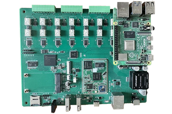
Differential traces should maintain consistent geometry throughout the routing path.
Avoid sharp 90-degree corners where possible. Use 45-degree routing or curved traces instead, particularly when routing high-speed differential signals.
The two traces should remain:
- Parallel whenever practical
- Similar in width
- Consistently spaced
- Referenced to the same plane
- As similar in length as possible
The spacing between the two traces should also be controlled according to the impedance target. A common layout guideline is to keep the differential-pair spacing relatively tight and consistent, often within approximately 2× the trace width depending on the required impedance and stackup.
For professional differential pair routing, the exact width and spacing should ultimately be determined from the PCB stackup and impedance calculation rather than relying on a universal spacing value.
3. Align Series Resistors and Capacitors With the Signal Path
When series resistors or capacitors are required in a differential signal path, their placement should be symmetrical.
For example, two components in a differential pair can be positioned vertically or horizontally in alignment with each other.
This helps maintain:
- Similar trace lengths
- Consistent routing geometry
- Balanced parasitic effects
- Better differential-mode signal integrity
Component placement should avoid forcing one side of the differential pair to take a significantly longer or more complicated route than the other.
4. Maintain Equal Length and Consistent Spacing
Differential pairs should be routed with matched lengths and consistent spacing whenever possible.
If one trace is significantly longer than the other, the two signals can arrive at different times. This creates differential skew and may degrade the quality of the received signal.
Length matching is particularly important for high-speed interfaces where the timing margin is limited.
The objective is not simply to make the two traces visually similar. The electrical path should also be as symmetrical as practical, including:
- Trace length
- Number of vias
- Via structure
- Layer transitions
- Trace width
- Trace spacing
- Reference-plane conditions
When routing a high-speed differential pair, maintaining symmetry is one of the most important principles of PCB impedance control.
5. Compensate for Differential Pair Length Mismatch
In practical PCB layouts, perfect length matching is not always possible.
Component pin locations, via positions, routing channels, and available board space can cause one trace to become longer than the other. If the mismatch becomes significant, it can introduce timing skew and increase common-mode conversion.
Therefore, length compensation should be applied where the mismatch occurs.
A commonly used design target is to keep the differential-pair length difference within approximately 5 mil for sensitive high-speed interfaces, although the actual requirement should be determined by the interface specification and timing budget.
A good compensation principle is:
Correct the mismatch as close as practical to where it occurs.
Avoid adding large, unnecessary serpentine sections at the end of the routing path simply to force the two traces to the same nominal length. Excessive meandering can increase coupling between adjacent trace segments and may negatively affect signal integrity.
How PCB Impedance Is Calculated
Controlled impedance depends on the physical structure of the PCB stackup. In practical engineering workflows, impedance calculators such as Polar Instruments’ Si9000 can be used to calculate the required trace geometry.
Typical parameters include the following.
| Parameter | Description |
|---|---|
| H1 | Dielectric thickness between the impedance trace and its reference layer |
| Er1 | Dielectric constant of the PCB material |
| W1 | Designed trace width |
| W2 | Actual or adjusted upper trace width after considering manufacturing compensation |
| S1 | Spacing between the two differential traces |
| T1 | Copper thickness |
| C1/C2/C3 | Solder mask thicknesses on the relevant PCB surfaces |
| CEr | Dielectric constant of the solder mask |
The dielectric constant varies depending on the actual PCB material and construction. Typical engineering calculations may use approximate values, but the manufacturer’s material data and stackup should be used whenever available.
For example, the source design reference uses approximately 4.2–4.6 for the PCB dielectric constant and approximately 3.5 for solder mask. These values are useful as calculation references but should not replace actual material specifications.
Why PCB Stackup Matters for Controlled Impedance
Trace width alone does not determine impedance.
A trace routed over a reference plane behaves differently depending on the distance between the trace and the plane. Therefore, the following stackup parameters must be considered together:
- Trace width
- Trace spacing
- Copper thickness
- Dielectric thickness
- Dielectric constant
- Reference-plane location
- Solder mask thickness
- Differential-pair geometry
For this reason, impedance-controlled routing should be performed using the actual PCB stackup instead of designing traces based solely on generic width rules.
A properly defined stackup also makes communication between the PCB designer and manufacturer much easier.
See PCB Design & Layout for more information about PCB layout and design-for-manufacturing considerations.
Common Problems in Multilayer PCB Impedance Routing
Several routing practices can create impedance discontinuities or differential signal problems.
Excessive Vias
Every via introduces parasitic capacitance and inductance. Excessive layer transitions can therefore affect signal integrity, especially at higher frequencies.
Keep the number of vias as low as practical and maintain a consistent via structure between the two traces.
Inconsistent Trace Spacing
If the spacing between differential traces changes significantly along the routing path, the coupling between the two traces also changes. This can affect differential impedance.
Maintain consistent spacing whenever possible.
Asymmetric Routing
One trace may pass around a via or component while the other takes a direct path. This creates different electrical environments for the two signals.
The solution is to maintain symmetrical routing and component placement.
Poor Reference-Plane Continuity
A high-speed trace should maintain a continuous reference plane beneath or adjacent to it.
If the reference plane is interrupted by a split, void, or inappropriate layer transition, the return current may need to take a longer path. This can increase electromagnetic radiation and cause impedance discontinuities.
Excessive Serpentine Compensation
Length matching is important, but excessive serpentine routing is not automatically better.
Closely spaced parallel segments of the same trace can couple to one another, increasing local capacitance and changing the effective impedance. Length compensation should therefore be designed carefully.
Manufacturing Considerations for Controlled Impedance PCB
Controlled impedance is not only a layout issue. Manufacturing tolerances also affect the final impedance of the PCB.
Important manufacturing variables include:
- Final trace width
- Copper thickness
- Dielectric thickness
- Etching compensation
- Lamination registration
- Material dielectric constant
- Solder mask thickness
- Layer-to-layer alignment
For this reason, the PCB designer should communicate the target impedance, impedance tolerance, stackup, reference layers, and critical signal nets to the manufacturer.
A professional PCB manufacturer can use the supplied stackup and design data to verify whether the specified impedance can be achieved before production.
Impedance Testing and Verification
After fabrication and assembly, critical high-speed boards may require electrical or impedance-related verification depending on the application.
For PCBA projects, electrical testing and functional testing can help identify manufacturing defects that could affect system performance.
See PCBA Testing for information about electrical and functional testing capabilities.
For high-reliability applications, impedance control should be treated as part of the complete quality-management process rather than as an isolated PCB layout requirement.
More information is available through Quality Management.
Key Takeaways
Successful controlled impedance PCB design requires coordination between schematic design, component placement, PCB layout, stackup definition, fabrication, and testing.
The most important practical rules are:
- Keep related components close together.
- Minimize unnecessary vias and layer transitions.
- Route differential pairs in parallel and symmetrically.
- Maintain consistent trace width and spacing.
- Keep differential-pair lengths closely matched.
- Compensate for length mismatch where it occurs.
- Use the actual PCB stackup for impedance calculations.
- Maintain continuous reference planes.
- Avoid excessive serpentine routing.
- Confirm impedance requirements with the PCB manufacturer before fabrication.
In high-speed multilayer boards, impedance control is ultimately a system-level engineering task. Good PCB design establishes the correct geometry, while controlled manufacturing processes ensure that the physical board remains close to the intended electrical characteristics.