HDI PCB Design Guide: BGA Routing and Multilayer Layout Rules
What HDI PCB Design Covers Today
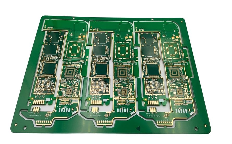
HDI PCB design means building boards that fit very dense circuits into a small area without sacrificing signal quality. High-density interconnect boards use finer lines, smaller vias, and more layers than ordinary boards, and they appear wherever processors, memory, and wireless circuits must work together in a compact product. The design decisions made at the layout stage decide whether those boards can be manufactured at reasonable cost and whether the signals inside them stay clean.
Many high-frequency and special signals leave integrated circuits through fine-pitch packages such as ball grid arrays. A large part of the routing challenge concentrates around those packages, so how the designer places the surrounding small components and how the traces leave the pads have a direct effect on the behavior of the whole board. This article explains the layout, routing, and stackup rules that keep an HDI design manufacturable and electrically sound.
Placement Rules That Decide Electrical Performance
Digital ground and analog ground should be separated, and reaching that goal starts with understanding the parts that generate interference. The designer must know which pins of an integrated circuit produce high-order harmonics from fast digital edges, which pins are sensitive to electromagnetic interference, and how the signal paths run inside the device. Overall placement is the first condition for good electrical performance, because components that radiate noise should sit close to their power supply, while weak-signal circuits should sit close to the signal input or sensor, where a short, clean path improves the signal-to-noise ratio for later processing.
Small components around a BGA are not equal in importance. Bypass capacitors, clock RC circuits, EMI damping circuits, and small power circuit groups for the chip must be placed as close to the package as possible, because their job depends on short connections. Ordinary pull resistors and small general-purpose circuits can sit slightly farther away. Ranking the small parts before placement makes the layout systematic and prevents the critical decoupling and filtering circuits from being pushed out of position by less important parts.
Trace Width, Skin Effect, and Data Bus Routing
Trace dimensions have to match the signal they carry. Wide copper suits low-frequency power and heavy current, but it is a poor choice for high-frequency signals, where the current crowds into the surface of the conductor. Because of this skin effect, high-frequency traces should be thin rather than wide and short rather than long, which also reduces coupling between adjacent circuits. Data signals appear on the board as fast pulses, and their high-order harmonic content decides whether the receiver reads the pattern correctly.
Uneven widths along a data bus are just as harmful as the wrong absolute width. If the traces in one bus lane differ in width, the signals arrive with different delays and the synchronization between them breaks. Serpentine routing exists mainly for this reason: it equalizes the path length inside a data bus so that every bit arrives at the receiver at nearly the same time. Keeping bus traces uniform in width, spacing, and length is one of the quiet fundamentals of a reliable high-density layout.
Copper pours add a second layer of protection. Large ground pours shield sensitive areas and reduce induced noise, and on double-sided boards the designer can use one side as a ground plane. Multilayer boards gain even more from internal power and ground planes, which act as natural shielding and isolation between the signal layers that carry the fast edges.
Ground Planes and the Multilayer Stackup
A sensible stackup puts the power planes in the middle and the signal layers on the outside. In a four-layer board, for example, the positive and negative power layers sit between the two outer signal layers, and no signal layer is placed between the power planes. This arrangement lets the planes work as filtering, shielding, and isolation, and it also helps the PCB factory control impedance, because the distance between each signal layer and its reference plane is short and uniform.
Mixed-signal boards need extra care where digital and analog circuits meet. Splitting the ground plane can help isolate noisy digital returns from sensitive analog returns, but the split must never be crossed by a trace that expects a continuous return path. When the analog and digital sections are separated by layout rather than by a hard cut in the plane, many noise problems disappear without the risks of a badly placed split.
BGA Fanout and Microvia Strategy
Routing around a ball grid array follows clear priorities. A bypass capacitor on the same side as the chip should connect directly from the chip pin to the capacitor and then to the via that reaches the plane, while a bypass on the opposite side may share the VCC and ground vias of the BGA, with a trace length no longer than about 100 mils. Clock RC circuits have requirements on width, spacing, and length, and their traces must be short, smooth, and free from crossings over supply splits.
Damping and EMI RC circuits need grouped, undisturbed routing. The traces should stay short and clean, one group at a time, and must not be mixed with unrelated signals, because the filtering they provide depends on controlled parasitics. Power circuit groups below forty mils, built from small capacitors, inductors, and resistors, sit near the chip and are separated from one another by the series parts that divide the supply rails.
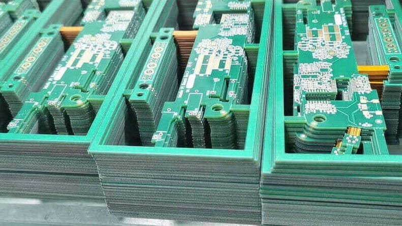
HDI manufacturing widens the routing options for dense packages. Microvias drilled with lasers connect outer layers without consuming the space of a through-hole, and blind and buried vias free the outer layers for routing while keeping inner layers connected. Fine-pitch BGAs that cannot be fanned out with through-holes on one layer become routable when a microvia drops to an inner layer and a short trace escapes between the pads. The via pattern, the pad size, and the chosen layer pairs must be agreed with the factory, because they determine the yield and the cost of the board.
Design for High-Volume Manufacturing
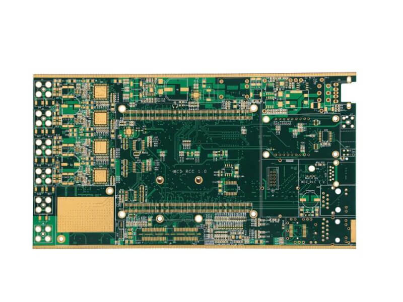
A design that works as a prototype may still be expensive in volume if the layout ignores the process. Controlled impedance requires the stackup, the trace width, and the plane spacing to be matched to the material and the manufacturing capability, so impedance values should be agreed with the factory early rather than discovered on the test report. Annular ring sizes, via diameters, and spacing rules should respect the capability table of the production line that will actually build the board.
Panelization and tooling add their own constraints. Features that must be routed, slots that need special milling, and board outlines with thin sections should be flagged during design review, because they affect panel strength and cost. When the design files include clear stackup notes, impedance requirements, and a net list that matches the schematic, the factory can quote accurately and start production without engineering loops.
Test features are part of good DFM for high-density boards. Impedance coupons placed on the production panel let the factory measure the actual trace impedance of the batch, and test points on every net make electrical testing possible without probing a fine-pitch pad. Even when space is tight, a designer should reserve room for these features, because verifying the board after production protects the customer from receiving a batch with silent signal-integrity problems.
In short, a successful HDI project combines disciplined placement, matched bus routing, a clean stackup, and an early conversation with the factory that will build the board.
How gopcb Helps with HDI Projects
gopcb reviews every high-density design before production. Our engineering team checks the stackup against the impedance targets, verifies that microvia and BGA fanout rules match our manufacturing capability, and returns clear feedback before the first panel is ordered. That review turns a good layout into a board that builds fast, tests clean, and performs as simulated.
The complete flow is available in one place: PCB manufacturing for multilayer and HDI fabrication, PCB design support for stackup and layout review, SMT PCB assembly for fine-pitch placement, PCBA testing for electrical verification, and PCB assembly services for the finished module. Send gopcb your design files to start an HDI project with a manufacturing check before you commit to volume.
The value of careful layout appears in the finished product rather than on the schematic. Two boards with identical components can behave completely differently when one was laid out with the current paths in mind and the other was not. Noise margins, timing, and electromagnetic emissions are decided by centimeters of copper, by the position of one capacitor, and by the way one return current crosses the board, which is why experienced design reviews spend as much time on placement as on routing.
Documentation completes the design. Stackup drawings, impedance tables, special note requirements, and a list of critical nets give the manufacturing team the same picture that the designer has. When those notes are missing, the factory has to guess, and a guess about a hundred-ohm differential pair or a thin core material can ruin an entire batch. A short, clear design-for-manufacturing sheet is the cheapest insurance an HDI project can buy.