How to Export PADS Gerber file: Complete PCB Guide
Why Correct Gerber File Export Matters
Gerber files are the primary manufacturing data used to convert a PCB design into physical circuit boards. Even when the PCB layout itself is correct, an incorrect or incomplete Gerber output can cause missing copper, incorrect solder mask openings, misaligned layers, or incorrect drilling information during fabrication.
Different PCB design software uses different procedures for generating manufacturing files. After reviewing Gerber output from Altium Designer, this guide focuses on the correct workflow for exporting a PADS Gerber file.
Before sending PCB fabrication data to a manufacturer, designers should always review the exported files and verify that every required layer is included and correctly aligned.
For additional information about manufacturing requirements, see PCB Manufacturing.
Step 1: Pour Copper Before Exporting Gerber Files
Before generating Gerber files, make sure all required copper pours have been properly updated.
In PADS, use the copper pour management function in the toolbar and select the appropriate copper-pour operation according to the PCB design.
If the design uses plane connections or copper areas, pay particular attention to whether all required regions have been successfully poured.
An incomplete copper pour can result in missing copper areas in the final Gerber output.
Before moving to the next step, verify:
- All copper areas have been poured.
- Plane connections are correct.
- No required copper region has been accidentally omitted.
- The copper pour reflects the latest PCB layout.
- No unintended isolated copper remains.
This step is especially important because the Gerber output represents the actual state of the PCB database at the time of export.
Step 2: Open the Gerber/CAM Output Manager
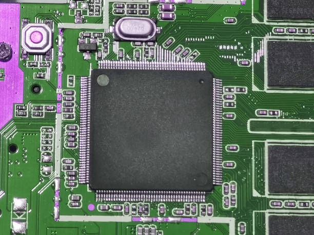
After completing the copper pour, open the CAM output functions in PADS.
The general workflow is:
File → CAM → Create Output Directory → Add Output Content
Create a dedicated output directory for the manufacturing files. Keeping all generated files in one controlled directory makes it easier to review the complete PCB fabrication files before sending them to the manufacturer.
A typical PCB Gerber package may contain:
- Top copper
- Bottom copper
- Inner copper layers
- Top solder mask
- Bottom solder mask
- Top silkscreen
- Bottom silkscreen
- Paste mask layers
- Board outline
- Drill drawing
- NC drill files
- HDI drill files
- Other required mechanical or special layers
The exact file set depends on the PCB structure and manufacturing requirements.
Step 3: Configure Copper Layer Output
When exporting copper layers, select the corresponding layers according to the PCB stackup.
The top, bottom, and inner copper layers should be exported separately.
One important point is to avoid placing unnecessary 2D drawing elements on the copper layers.
If 2D lines are being used for documentation rather than actual copper features, they should not be included in the routing-layer Gerber output. Otherwise, the manufacturer may interpret those lines as actual PCB copper.
Inner-Layer Output
For inner layers, use the appropriate CAM plane output method when the layer is defined as a negative plane.
The output method should correspond to how the PCB layer is actually constructed in the design.
Include the Board Outline
The board outline should be included where required for layer registration and manufacturing reference.
A consistent board outline helps the manufacturer align different Gerber layers correctly.
After configuring each layer, use the preview function to verify the output.
Check that:
- The copper pattern is complete.
- No unrelated drawing elements are present.
- Pads and traces are in the correct positions.
- The board outline is correctly displayed.
- Layer polarity is correct.
- The layer is correctly aligned with the PCB dimensions.
If special design elements exist on other layers, make sure those layers are also selected for output.
For professional PCB design, the final Gerber package should always be reviewed rather than being sent directly to fabrication without verification.
Step 4: Export Silkscreen Layers
The silkscreen layers contain component references, polarity markings, logos, labels, and other identification information.
When exporting the top or bottom silkscreen, select the appropriate silkscreen layer and configure the required output elements.
As with other PCB layers, preview the output before generating the final file.
Pay attention to:
- Reference designators
- Polarity indicators
- Component labels
- Logos
- Text size
- Text location
- Board outline
- Overlapping pads or solder mask openings
Silkscreen information should not unintentionally overlap critical soldering areas or other manufacturing features.
Step 5: Export Paste Mask and Solder Mask
Paste mask and solder mask are separate manufacturing layers and should not be confused.
Paste Mask
The paste mask defines the areas where solder paste is deposited during SMT assembly.
It is primarily used to manufacture the stencil and control solder paste application.
Solder Mask
The solder mask defines areas where the protective solder mask coating is opened to expose copper pads and other required conductive areas.
For conventional output, the relevant mask layers should be configured correctly and the board outline should be included where required.
Always use the preview function to confirm that the mask openings correspond to the intended PCB pads.
Incorrect solder mask output can cause problems such as:
- Covered pads
- Oversized openings
- Insufficient clearance
- Incorrect component land patterns
- Assembly defects
For more information about PCB fabrication and assembly requirements, see PCB Capabilities.
Step 6: Configure the Drill Drawing
The drill drawing provides a visual representation of the PCB’s drilling information.
Before generating the drill drawing, check whether the drill table overlaps the PCB layout.
If the drill table is placed directly over the board graphics and interferes with the drawing, adjust its position.
The general process is:
- Enter the required coordinate or offset values.
- Confirm the new position.
- Preview the drill drawing.
- Verify that the drill table no longer overlaps important PCB graphics.
- Confirm the final position.
- Add the board outline in the layer configuration if required.
- Generate the final drill drawing.
The drill drawing is primarily a visual reference, while the actual drilling data is normally provided through NC drill files.
Step 7: Export NC Drill Files for Through-Holes
NC drill files contain the actual drilling information required for PCB fabrication.
For conventional through-hole drilling, select the appropriate drill output function and generate the NC drill file.
Before sending the file to the manufacturer, verify:
- Drill sizes
- Hole locations
- Plated and non-plated hole requirements
- Drill quantity
- Board coordinates
- Units
- Coordinate format
- Drill file completeness
The drill data must correspond precisely to the PCB layout and the associated manufacturing documentation.
A mismatch between the Gerber layers and drill files can result in incorrectly positioned holes or manufacturing delays.
Step 8: Export HDI Drill Files
HDI boards require more detailed drilling information because different microvia structures can connect different layer combinations.
Before exporting HDI drill files, configure the corresponding start and end layers for each drill structure.
For example, different drill files may be required for different layer transitions depending on the HDI stackup.
The general process is:
- Define the required start and end layers.
- Configure the corresponding HDI drilling parameters.
- Select the appropriate drill layer pair.
- Export each required drill file separately.
- Review the generated files.
- Confirm that the drilling information matches the HDI stackup.
HDI manufacturing requires accurate coordination between the PCB layout, stackup, microvia structure, and drill data.
For complex multilayer and HDI boards, clear manufacturing documentation is especially important.
Step 9: Review the Complete Gerber Package
Generating the files is not the final step.
Before submitting the Gerber file export package for production, perform a complete visual and technical review.
At minimum, check:
Layer Completeness
Make sure every required layer has been exported.
Layer Alignment
Verify that top, bottom, inner layers, solder mask, silkscreen, and drill data align correctly.
Board Outline
Confirm that the board dimensions and outline are correct.
Copper Features
Check traces, pads, planes, and copper areas for missing or unexpected features.
Drill Data
Verify that drill locations and sizes correspond to the PCB design.
Polarity
For negative inner-plane layers, confirm that the layer polarity has been configured correctly.
Special Layers
Check whether any mechanical, impedance, fabrication, or other special layers contain information required by the manufacturer.
A Gerber viewer can be used to inspect the complete manufacturing package before release.
Common Gerber Export Problems
Several common mistakes can cause problems during PCB fabrication.
Missing Copper Pour
If the copper pour is not updated before export, the Gerber file may contain incomplete copper areas.
2D Drawing Lines Included in Copper Layers
Documentation lines accidentally included in copper output can be interpreted as real copper features.
Incorrect Layer Polarity
Incorrect polarity settings can completely change the appearance and interpretation of an inner plane layer.
Missing Board Outline
Without a clear board outline, layer registration and fabrication interpretation can become more difficult.
Incorrect Drill Data
The drill file must match the PCB design, including hole sizes, locations, and layer connectivity.
Missing HDI Drill Information
HDI boards often require multiple drill structures. Omitting one of the required drill files can make the manufacturing data incomplete.
Gerber Files and PCB Manufacturing
Gerber generation is the bridge between PCB design data and physical manufacturing.
A correct PADS Gerber file package should accurately communicate:
- PCB layer structure
- Copper patterns
- Solder mask openings
- Silkscreen information
- Paste mask information
- Board dimensions
- Drilling information
- HDI structures
- Other manufacturing requirements
However, Gerber files are only one part of a complete PCB manufacturing data package. Depending on the project, additional information such as fabrication drawings, stackup specifications, impedance requirements, material requirements, and assembly documentation may also be necessary.
For complex boards, designers should review the complete manufacturing package together rather than checking individual files in isolation.
Final Checklist for PADS Gerber Export
Before sending the files to a PCB manufacturing partner, use the following checklist:
- Copper pours have been updated.
- All copper layers have been exported.
- Inner-plane polarity is correct.
- 2D documentation lines are not incorrectly included in copper layers.
- Board outline is correct.
- Silkscreen layers have been reviewed.
- Solder mask layers have been reviewed.
- Paste mask layers have been reviewed.
- Drill drawing has been checked.
- NC drill files have been generated.
- HDI drill files have been configured and exported when required.
- All layers are correctly aligned.
- Gerber files have been visually inspected.
- Drill data matches the PCB layout.
- Special manufacturing layers are included when required.
Conclusion
Correct Gerber generation is an essential step between PCB layout and physical fabrication. A reliable Gerber file export workflow should include copper-pour verification, layer configuration, board-outline control, solder mask and silkscreen checks, drill-file generation, HDI drill configuration, and final Gerber inspection.
For complex multilayer or HDI boards, the designer should pay particular attention to layer polarity, drill structures, layer alignment, and manufacturing documentation.
Taking a few minutes to verify the complete Gerber package before release can prevent incorrect fabrication data from becoming an expensive PCB manufacturing problem.