Essential PCB Design Basics Every Engineer Should Know
A reliable printed circuit board starts with a solid understanding of fundamental design principles. PCB design is not simply about connecting components with traces. Layer stack-up, power distribution, grounding, signal return paths, component placement, routing, and manufacturing requirements must all work together.
For complex systems such as FPGA, DSP, high-speed digital, mixed-signal, and multilayer boards, mistakes made during schematic or layout development can lead to signal-integrity problems, EMI, power instability, and difficult debugging.
The following PCB Design Basics provide a practical foundation for developing reliable and manufacturable PCBs.
1. Verify FPGA Pin Assignments Before Schematic Design
When a circuit includes an FPGA, pin assignments should be verified before completing the schematic.
Certain FPGA pins have dedicated functions and may not be available as general-purpose I/O. Depending on the FPGA family, special pins may be associated with configuration, clocks, power, JTAG, differential interfaces, or other dedicated functions.
Therefore, engineers should use the FPGA vendor’s design tools to validate pin assignments before committing to the schematic.
For example, when using Intel FPGAs, Quartus Prime can be used to verify device pin assignments and related constraints.
This early verification can prevent major PCB redesigns caused by incompatible pin assignments.
2. Understand Multilayer PCB Stack-Up
PCB layer arrangement has a major influence on routing, power integrity, signal integrity, and EMI performance.
A typical four-layer PCB may use the following arrangement:
Layer 1: Signal
Layer 2: Ground
Layer 3: Power
Layer 4: Signal
A six-layer PCB may use a structure such as:
Layer 1: Signal
Layer 2: Ground
Layer 3: Signal
Layer 4: Signal
Layer 5: Power
Layer 6: Signal
The exact stack-up should be determined according to routing density, impedance requirements, operating frequency, power distribution, and manufacturing capability.
For high-speed designs, signal layers should generally be placed close to continuous reference planes. This provides a predictable return-current path and helps reduce electromagnetic coupling.
A well-engineered PCB Stackup is therefore one of the foundations of high-speed PCB performance.
For complex multilayer, HDI, high-speed, and controlled-impedance boards, professional stack-up planning should be completed before routing. PCB Design & Layout Services
3. Use Internal Layers Efficiently
For boards with six or more layers, internal layers can provide valuable routing and reference-plane resources.
Whenever possible, high-speed signals should be routed on layers adjacent to ground or other suitable reference planes. Routing critical signals directly through power or ground planes should be avoided because doing so can fragment the reference plane and create unexpected return-current paths.
A practical multilayer strategy is to assign each layer a clear purpose:
- High-speed signal routing
- General signal routing
- Ground reference
- Power distribution
- Sensitive analog routing
- Dedicated interfaces
The goal is not simply to maximize the number of routing layers. The stack-up should create a controlled electromagnetic environment for the signals.
4. Plan Multiple Power Rails Carefully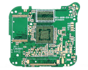
Complex FPGA and DSP systems often require several voltage rails.
For example, a system may contain:
- 5 V input or system power
- 3.3 V main logic power
- 1.8 V auxiliary power
- 1.2 V core power
Each voltage domain should be considered separately during PCB layout.
Use Copper Areas for Widely Distributed Power
A power rail that supplies many areas of the PCB can be difficult to route efficiently using narrow traces.
Where appropriate, copper pours or dedicated power planes can provide lower-impedance current paths and simplify distribution.
For example, a 3.3 V rail used throughout a board may benefit from a dedicated power plane or large copper region.
A 5 V input rail may only need to cover a relatively small area and can often be implemented using a sufficiently wide trace or copper region, depending on current requirements.
Keep Core Power Domains Compact
Low-voltage FPGA and processor core rails such as 1.2 V and 1.8 V often supply specific groups of devices.
Instead of routing these rails across the entire board, it can be advantageous to keep the relevant components physically close together and connect them using appropriately sized copper areas.
This is particularly useful around BGA devices, where routing space is limited.
The correct solution depends on current requirements, voltage-drop limits, thermal constraints, and the PCB stack-up.
5. Use Cross-Layer Routing Carefully
When signals are routed on adjacent layers, changing the dominant routing direction can reduce long parallel trace segments.
For example:
- Layer 1: primarily horizontal
- Layer 3: primarily vertical
- Layer 4: primarily horizontal
- Layer 6: primarily vertical
This approach can reduce broadside or edge-coupled parallel routing between layers.
However, routing direction alone does not guarantee good signal integrity. Trace spacing, reference-plane continuity, dielectric thickness, signal rise time, and interface speed must also be considered.
For high-speed interfaces, the primary objective is to maintain controlled impedance and a continuous return path.
6. Separate Sensitive Analog and Digital Circuits
Mixed-signal PCB design requires careful management of analog and digital circuits.
Sensitive analog components should generally be separated from noisy digital devices and high-current switching circuits.
However, simply dividing the PCB into an “analog half” and a “digital half” is not always sufficient.
A better approach is to understand where currents flow and ensure that noisy digital return currents do not pass through sensitive analog reference regions.
Use Controlled Grounding
Analog ground and digital ground should be managed according to the circuit architecture and the data converter or device manufacturer’s recommendations.
Depending on the system, analog and digital domains may be connected at a controlled location rather than being completely isolated.
Ferrite beads or inductors may sometimes be used between power domains, but they should not be treated as a universal solution.
The component impedance characteristics, current level, frequency range, and return-current path must be evaluated before using them.
Good PCB Layout should control current paths rather than simply separating components by physical location.
7. Treat PCB Design as an Iterative Engineering Process
PCB design should be treated as an iterative process rather than a one-time conversion from schematic to layout.
A practical workflow is:
Step 1: Check the Schematic
Verify:
- Component connections
- Power pins
- Ground pins
- Net names
- Critical interfaces
- Differential pairs
- Clock signals
- Power domains
Power and ground connections deserve particular attention because errors in these networks can affect the entire system.
Step 2: Verify PCB Footprints
Every PCB footprint should be checked against the actual component package.
Verify:
- Pin numbering
- Pad dimensions
- Pad spacing
- Package orientation
- Courtyard
- Assembly requirements
- Thermal pads
- Mechanical dimensions
Incorrect footprints can cause expensive assembly and prototype problems.
Step 3: Import the Netlist
After schematic and footprint verification, transfer the design into the PCB layout environment.
At this stage, component placement may reveal problems in the original schematic, such as inconvenient pin assignments or unnecessarily long connections.
The schematic and PCB should therefore be reviewed together throughout the design process.
Step 4: Place Components
Component placement should consider:
- Signal flow
- Power flow
- Thermal requirements
- High-speed interfaces
- Connector positions
- Mechanical constraints
- Serviceability
The placement stage has a major impact on the eventual routing quality.
Step 5: Route and Review
Route critical power and signal networks first, then complete the remaining connections.
After routing, perform design-rule checks and review critical signal paths manually.
For complex designs, professional PCB Design & Layout services can help optimize component placement, multilayer stack-up, impedance control, and manufacturability.
8. Keep Crystal Oscillators Close to the IC
Crystal oscillators and other clock-generation components are sensitive to parasitic effects and unwanted coupling.
The crystal should generally be placed close to the corresponding IC pins, with short connections.
Avoid routing unrelated signals beneath or immediately around the crystal when the device manufacturer’s layout recommendations prohibit it.
A local ground reference can also help isolate sensitive clock circuitry from surrounding noise.
Use Controlled Clock Routing
When the same clock needs to reach multiple devices, the routing topology should be selected according to the clock frequency, edge rate, load, and timing requirements.
Possible approaches include:
- Point-to-point routing
- Star routing
- Daisy-chain routing
- Buffered clock distribution
- Dedicated clock-tree structures
For high-speed clocks, the routing topology should be determined through signal-integrity analysis rather than relying on a single universal routing rule.
9. Connector Pin Assignment Affects PCB Routing
Connector pin assignment has a surprisingly large influence on PCB routing complexity.
Poor signal ordering can force traces to cross repeatedly, increase routing length, and complicate differential-pair routing.
Therefore, connector pin assignments should be considered together with PCB placement and routing.
When possible, organize connector signals according to:
- Signal groups
- Differential pairs
- Power
- Ground
- High-speed interfaces
- Low-speed interfaces
- Return-current requirements
For high-speed connectors, placing ground pins strategically between noisy or high-speed signals can also help reduce coupling.
10. Design Board-to-Board Connectors for Easy Routing
When two boards are connected through board-to-board connectors, connector pin mapping should be planned together with the physical orientation of the boards.
For ribbon cables, corresponding interfaces can often use the same pin order.
For vertically stacked or mirrored board-to-board connectors, pin assignments may need to be mirrored depending on the physical orientation of the boards.
The objective is to make the signal paths as direct as possible and reduce unnecessary trace crossings.
However, connector pin mapping should always be determined by the actual mechanical arrangement rather than following a rigid rule.
11. Optimize Module-to-Module Signal Connections
When two modules are placed on the same side of a PCB, mirrored signal assignments can sometimes simplify routing.
When modules are located on opposite sides of the board, a different pin-mapping strategy may be more efficient.
For example, the following factors should be considered:
- Physical orientation
- Pin numbering
- Signal direction
- Connector location
- Routing layer
- Differential-pair requirements
- Return-current path
There is no universal pin-ordering rule. The best approach is the one that minimizes unnecessary crossings while preserving electrical requirements.
12. Minimize Power and Ground Loop Area
The physical area enclosed by a power and ground current loop directly affects its susceptibility to electromagnetic coupling.
A large loop can behave as an effective antenna and increase EMI sensitivity and radiation.
A better layout keeps the power and return paths close together.
For example, instead of routing power and ground along opposite sides of a board, keep the supply and return paths physically close wherever practical.
Reducing loop area can significantly improve EMI Control.
This principle applies not only to power networks but also to high-speed signal paths.
For high-speed signals, the forward current and return current should remain closely coupled through an adjacent reference plane.
13. Reduce Parallel Signal Routing
Long parallel traces can increase mutual capacitance and inductive coupling between signals.
This can result in:
- Crosstalk
- Ringing
- Timing errors
- Overshoot and undershoot
- Increased EMI
Where possible, avoid long parallel routing between sensitive signals.
Increasing trace spacing, changing routing direction, using different routing layers, and maintaining appropriate reference-plane structures can all help reduce coupling.
The required spacing should be determined according to the signal rise time, stack-up, trace geometry, and interface requirements.
14. Validate the PCB Before Manufacturing
Before sending a design to fabrication, perform a comprehensive design review.
At minimum, verify:
Schematic
- Component values
- Power connections
- Ground connections
- Net names
- FPGA pin assignments
- Critical interfaces
PCB Layout
- Component placement
- Trace width
- Trace spacing
- Via sizes
- Differential pairs
- Reference planes
- Power distribution
- Ground continuity
Signal Integrity
- Controlled impedance
- High-speed return paths
- Clock routing
- Crosstalk
- Layer transitions
EMI
- Current-loop area
- Ground continuity
- Plane splits
- High-speed routing
- Sensitive analog regions
- Power distribution
Manufacturing
- PCB dimensions
- Layer stack-up
- Copper thickness
- Minimum trace/space
- Drill sizes
- Via structures
- Solder mask
- Surface finish
A professional DFM review before fabrication can identify potential manufacturing and electrical problems while changes are still inexpensive.
For advanced PCB projects, GOPCBA provides PCB fabrication, multilayer PCB manufacturing, controlled impedance, HDI, high-speed PCB, and other advanced manufacturing capabilities. PCB Manufacturing Services
15. Why Good PCB Design Starts with Fundamentals
Many PCB failures are not caused by a single complicated technical issue. They often originate from basic problems such as incorrect pin assignments, poor component placement, unsuitable stack-up, discontinuous return paths, excessive trace length, or poorly designed power distribution.
A reliable PCB should therefore be designed as an integrated electrical and mechanical system.
The most important PCB Design Basics include:
- Verify device pin assignments before schematic completion.
- Select the layer stack-up according to signal and power requirements.
- Keep high-speed signals close to continuous reference planes.
- Use appropriate copper areas or planes for widely distributed power.
- Keep sensitive analog and noisy digital circuits appropriately separated.
- Place crystals and clock components close to their associated ICs.
- Optimize connector pin assignments before routing.
- Keep power and return paths close together.
- Minimize high-speed loop area.
- Avoid unnecessarily long parallel traces.
- Check signal integrity and manufacturability before fabrication.
Ultimately, high-quality PCB Layout is about controlling current paths, electromagnetic coupling, impedance, and physical geometry at the same time.
When these principles are incorporated from the beginning, engineers can build boards with better Signal Integrity, lower EMI Control risk, and greater manufacturing reliability.