PCBA Soldering Problems: 6 Common Causes and Practical Solutions
Poor solderability is one of the most common problems encountered during PCBA Soldering. When solder does not properly wet a PCB pad or component lead, the result may be an open circuit, weak solder joint, intermittent connection, or complete assembly failure.
These problems can increase rework, reduce production efficiency, and affect delivery schedules.
Importantly, poor soldering is rarely caused by a single factor. PCB design, component condition, solder paste, process parameters, equipment accuracy, and post-soldering cleaning can all influence solder joint quality.
Understanding the root causes makes it easier to prevent defects before they reach final inspection.
6 Common Causes of Poor Solder Wetting in PCBA
1. Improper PCB Pad Design
The solder pad is the foundation of a reliable solder joint.
If pad dimensions, shape, spacing, or component footprints are not properly designed, solder may fail to form a sufficient connection.
Common design-related problems include:
- Pads that are too small or narrow
- Incorrect component footprints
- Insufficient pad spacing
- Poor thermal relief design
- Improper pad-to-lead alignment
- Oxidized or contaminated PCB surfaces
Design-for-manufacturing analysis should be performed before production to identify potential assembly problems.
A professional PCB Design & Layout review can help optimize footprints, pad geometry, component spacing, and other design details that affect solderability.
2. Oxidized or Contaminated Component Leads
Component leads must have a clean and solderable surface for reliable solder joint formation.
Oxidation, damaged plating, contamination, moisture, or improper storage can reduce solderability.
Potential causes include:
- Long-term storage
- High humidity
- Corrosive environments
- Damaged surface plating
- Poor-quality or improperly handled components
When the metal surface is heavily oxidized, solder may fail to wet the lead even when the soldering process itself is properly controlled.
For this reason, component inspection and proper material storage are important parts of PCBA Manufacturing.
3. Improper Solder Paste or Flux
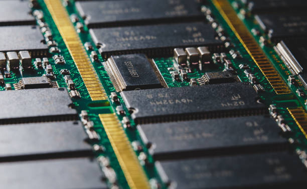
Solder paste plays a critical role in SMT soldering.
If the solder paste is expired, improperly stored, contaminated, or unsuitable for the application, soldering performance may deteriorate.
Important factors include:
- Solder paste alloy
- Powder particle size
- Flux activity
- Storage temperature
- Storage duration
- Paste viscosity
- Environmental humidity
For fine-pitch components, an appropriate solder paste particle size is especially important.
Flux must also remain sufficiently active to remove surface oxides and promote proper solder wetting.
Poor solder paste management can therefore lead to defects such as insufficient solder, non-wetting, solder bridging, and weak joints.
4. Incorrect Soldering Process Parameters
Even when the PCB and components are in good condition, incorrect process parameters can cause soldering defects.
Reflow Soldering Problems
For SMT production, the reflow temperature profile must be carefully controlled.
An unsuitable profile can result from:
- Excessively rapid heating
- Insufficient preheating
- Inadequate soaking
- Insufficient time above liquidus
- Excessive peak temperature
- Improper cooling rate
For example, insufficient thermal exposure may prevent the solder from fully melting and wetting the pad and component termination.
Excessive heating, however, can damage components or PCB materials.
Wave and Selective Soldering Problems
Through-hole assemblies require additional process considerations.
During wave soldering or selective soldering, insufficient preheating, inappropriate solder temperature, poor flux application, or incorrect contact time can affect solder flow and wetting.
For assemblies containing both SMT and through-hole components, the soldering process must be coordinated across different assembly stages.
GOPCBA supports Through-Hole PCB Assembly for projects requiring reliable integration of through-hole components into the overall PCB assembly process.
5. Equipment Accuracy and Process Stability
Manufacturing equipment can also contribute to poor soldering.
For SMT production, placement accuracy directly affects the alignment between component terminals and PCB pads.
Potential equipment-related problems include:
- Component placement offset
- Excessive component rejection
- Inaccurate solder paste printing
- Reflow temperature instability
- Poor equipment calibration
- Mechanical wear
Solder paste printing is particularly important because the printed paste volume and position determine how much solder is available for each joint.
Regular equipment maintenance, calibration, and process monitoring help maintain consistent production quality.
6. Improper Cleaning After Soldering
Cleaning is another factor that is sometimes overlooked.
Depending on the flux system and product requirements, PCB assemblies may or may not require cleaning.
Problems can occur when cleaning is either excessive or inadequate.
Excessive Cleaning
An aggressive cleaning process or incompatible cleaning chemical can potentially affect component materials, markings, coatings, or other assembly features.
Insufficient Cleaning
Remaining flux residues or contaminants may affect the long-term reliability of the assembly, particularly in applications with demanding electrical or environmental requirements.
The cleaning process should therefore be selected according to the solder paste or flux chemistry, PCB materials, components, and final product requirements.
How to Troubleshoot PCBA Soldering Defects
When solder does not properly wet a pad or component lead, troubleshooting should follow a systematic process rather than immediately changing the reflow temperature.
Step 1: Inspect the PCB
Check the PCB pads for:
- Oxidation
- Contamination
- Damaged surface finish
- Incorrect dimensions
- Manufacturing defects
The PCB surface finish should be compatible with the intended assembly process.
Step 2: Check Component Condition
Inspect component leads and terminations for oxidation, contamination, damaged plating, and storage-related issues.
If multiple components from the same lot show poor solderability, material quality or storage conditions should be investigated.
Step 3: Verify Solder Paste
Check the solder paste’s:
- Expiration date
- Storage conditions
- Particle size
- Alloy
- Viscosity
- Flux activity
Solder paste should be handled according to the manufacturer’s specifications.
Step 4: Review the Thermal Profile
Measure the actual reflow profile instead of relying only on the oven’s programmed settings.
Compare the measured profile with the solder paste manufacturer’s recommended process window.
Step 5: Check Placement and Printing
Inspect solder paste deposition and component placement.
An offset component or insufficient paste volume can produce defects even when the reflow profile is correct.
Step 6: Analyze the Solder Joint
Inspection technologies such as AOI and X-ray can help identify soldering problems that are difficult to detect visually.
For hidden joints such as BGA connections, X-ray inspection can provide additional information about solder coverage and joint formation.
How to Prevent Soldering Defects During PCBA Manufacturing
The most effective approach is to prevent defects before production rather than relying entirely on final inspection.
Design for Manufacturability
A proper DFM review can identify PCB design issues before they become production problems.
Engineers should review:
- Component footprints
- Pad dimensions
- Component spacing
- Thermal design
- Solder mask openings
- Component orientation
- Test-point accessibility
Control Materials
PCB materials, components, solder paste, and flux should be stored and handled according to their specifications.
Moisture and oxidation control are particularly important for maintaining solderability.
Standardize the Soldering Process
Production should use controlled soldering profiles and documented process parameters.
Reflow, wave soldering, and selective soldering should each have defined operating conditions appropriate to the PCB and materials.
Use In-Process Inspection
Inspection should be performed throughout the assembly process.
Depending on the product, this may include:
- Solder Paste Inspection (SPI)
- Automated Optical Inspection (AOI)
- X-ray inspection
- Visual inspection
- Electrical testing
- Functional testing
These inspection methods can help identify defects earlier and reduce unnecessary rework.
Why Integrated PCB Assembly Helps Improve Soldering Quality
Soldering quality depends on the interaction between design, materials, equipment, and process control.
When PCB manufacturing, component sourcing, SMT assembly, through-hole assembly, inspection, and testing are coordinated within a single manufacturing workflow, potential issues can be identified earlier.
For prototype and low-volume products, this is particularly valuable because design and process adjustments can be made before production volumes increase.
GOPCBA’s Rapid PCBA Prototyping services can support early design validation and assembly process optimization before larger-scale manufacturing.
Conclusion
Poor solder wetting and soldering defects can originate from many different sources. PCB pad design, component oxidation, solder paste condition, thermal profiles, equipment accuracy, and cleaning processes all need to be considered when troubleshooting a failed solder joint.
The key to reliable SMT Assembly and PCBA Manufacturing is not simply increasing soldering temperature or changing solder materials. Instead, manufacturers should establish a controlled process that begins with manufacturable PCB design and continues through material management, soldering, inspection, and testing.
By identifying potential problems early and applying systematic process control, manufacturers can reduce soldering defects, minimize rework, and achieve more consistent PCB assembly quality.