SMT PCB Assembly to DIP Quality Control: Complete Guide
In electronics manufacturing, consistent quality depends on much more than a single inspection step. A small placement error during SMT or an incomplete solder joint during DIP assembly can lead to electrical failures, rework, production delays, and even field failures.
A reliable PCB Assembly process therefore requires quality control throughout the entire manufacturing workflow, from design review and material preparation to SMT placement, soldering, DIP assembly, inspection, and final testing.
For manufacturers handling complex electronics, integrating engineering review, automated inspection, process monitoring, and traceability is essential for maintaining stable production quality.
SMT PCB Assembly: Building the First Quality-Control Barrier
SMT is one of the most precision-sensitive stages in electronics manufacturing. Components are placed directly onto PCB pads, often at very small pitches and high component densities. Placement accuracy and soldering quality have a direct impact on overall assembly yield.
A well-controlled SMT PCB Assembly process typically combines automated production equipment with multiple inspection technologies.
Precision Placement and Reflow Soldering
The SMT process generally includes solder paste printing, component placement, and reflow soldering. Each stage must be carefully controlled to prevent defects such as insufficient solder, solder bridging, component misalignment, tombstoning, and poor wetting.
Solder paste printing is particularly important because paste volume and position determine the quality of the subsequent solder joints. Stencil design, printing pressure, squeegee speed, paste condition, and PCB surface quality all influence the result.
After component placement, the PCB enters the reflow oven. The thermal profile must be matched to the solder paste and component requirements to ensure reliable solder joint formation while avoiding excessive thermal stress.
For projects requiring both surface-mount and through-hole components, mixed-technology PCB assembly can integrate multiple assembly technologies into a coordinated manufacturing process.
SPI, AOI, and X-Ray Inspection
Automated inspection provides critical feedback during SMT production.
SPI (Solder Paste Inspection) measures solder paste deposition before components are placed. It can identify problems such as insufficient paste, excessive paste, offset printing, and uneven deposition.
AOI (Automated Optical Inspection) checks component position, polarity, soldering appearance, and other visible defects after placement and reflow.
For hidden solder joints, such as those beneath BGA packages, X-Ray inspection provides internal visibility that optical inspection cannot achieve. It can help identify solder voids, bridging, insufficient solder, and other hidden defects.
Using multiple inspection technologies creates a layered quality-control system rather than relying on a single inspection method.
DIP PCB Assembly: Controlling Through-Hole Soldering Quality
DIP and other through-hole components remain important in many electronic products, particularly applications requiring mechanically robust connections, larger components, connectors, transformers, or high-current interfaces.
A controlled DIP PCB Assembly process typically includes component insertion, soldering, inspection, cleaning, and functional testing.
Standardized Through-Hole Assembly
Component insertion must follow the approved BOM, assembly drawings, polarity requirements, and production instructions. Incorrect component orientation or insertion can cause functional failures even when the solder joints themselves appear acceptable.
Depending on the PCB design, through-hole soldering may use wave soldering, selective soldering, or manual soldering.
Wave soldering is suitable for boards containing a large number of compatible through-hole joints, while selective soldering provides more localized control for assemblies where certain components or sensitive areas cannot pass through a conventional wave-soldering process.
For assemblies with a significant number of through-hole components, through-hole PCB assembly provides a dedicated manufacturing approach for reliable mechanical and electrical connections.
Inspection and Functional Testin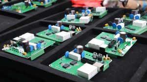
Visual inspection remains useful for identifying visible soldering problems, incorrect component orientation, damaged components, and workmanship issues.
However, visual inspection alone cannot verify whether an electronic assembly functions correctly. Functional testing can simulate operating conditions and verify whether the completed board performs according to its intended electrical requirements.
Depending on the product, testing may include continuity testing, in-circuit testing, functional testing, power-up testing, or application-specific verification.
Quality Control Must Cover the Entire Manufacturing Process
High-quality PCB assembly cannot be achieved by inspecting finished boards alone. Defect prevention should begin before production starts.
A complete quality system connects design review, materials, manufacturing processes, inspection, testing, and traceability.
DFM Review Before Production
Many manufacturing problems originate from PCB design rather than the production line.
Design features such as insufficient component spacing, unsuitable pad dimensions, difficult soldering areas, thermal imbalance, inadequate clearances, and poor component accessibility can increase manufacturing risk.
A DFM review identifies these potential problems before fabrication and assembly begin. This allows engineers to modify the design while changes are still relatively easy and inexpensive.
Using professional PCB design and layout services can help optimize PCB layouts for manufacturability, assembly reliability, component placement, and production efficiency.
Material and Component Control
Quality also starts with incoming materials.
PCB substrates, solder paste, electronic components, and other production materials should be verified against the approved specifications. Proper storage conditions are also important because moisture, oxidation, contamination, and improper handling can affect solderability and component reliability.
For turnkey manufacturing projects, component sourcing and material management should be integrated with production planning. component procurement services can help coordinate component purchasing with the PCB assembly process and reduce supply-chain-related production risks.
Traceability and Process Monitoring
Modern electronics manufacturing increasingly relies on digital production records to improve traceability.
A robust traceability system can associate production information with individual PCB assemblies or manufacturing batches. Depending on the production system, records may include component lot information, machine parameters, inspection results, operator information, and testing data.
This information becomes particularly valuable when a defect is discovered. Engineers can use production records to identify affected batches, analyze potential causes, and implement corrective actions more efficiently.
Process monitoring also allows manufacturers to detect trends before they develop into large-scale quality problems.
Four Key Factors Behind Reliable PCBA Quality
Consistent manufacturing quality is usually the result of several systems working together rather than one isolated technology.
1. Engineering Prevention
Design-for-manufacturing analysis should identify potential production risks before the PCB reaches the production line.
2. Automated Process Control
Automated placement, soldering, SPI, AOI, and X-Ray inspection can reduce process variation and improve defect detection.
3. Testing and Verification
Electrical and functional testing provides another layer of protection by confirming that assembled boards operate as required.
4. Continuous Improvement
Production data and inspection results should be analyzed continuously. Repeated defects should trigger root-cause analysis and corrective action rather than simply being repaired after production.
For companies developing new electronic products, rapid PCBA prototyping can also help identify manufacturing and design issues during the prototype stage, before products move into larger-scale production.
Why Integrated SMT and DIP Manufacturing Matters
Modern electronic products often combine surface-mount and through-hole components. Managing SMT and DIP separately can create additional communication, scheduling, and quality-control challenges.
An integrated manufacturing workflow connects:
- PCB design and DFM review
- Component sourcing
- SMT placement
- Reflow soldering
- Through-hole assembly
- Wave or selective soldering
- AOI, SPI, and X-Ray inspection
- Functional testing
- Final assembly and quality verification
This approach creates better process continuity and reduces the risk of information gaps between manufacturing stages.
Conclusion
Achieving consistent quality from SMT through DIP requires a complete manufacturing strategy rather than a single inspection procedure.
Precision component placement, controlled soldering, automated inspection, functional testing, material management, DFM review, and production traceability all contribute to reliable PCBA Quality Control.
For electronics manufacturers, choosing an integrated PCB Assembly Manufacturing partner with SMT, through-hole, inspection, testing, engineering, and production capabilities can simplify the manufacturing process while improving consistency and scalability.
GOPCBA provides integrated PCB and PCBA manufacturing services covering prototype development, PCB assembly, component sourcing, testing, and production support for a wide range of electronic applications.