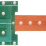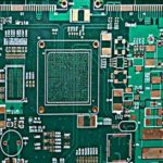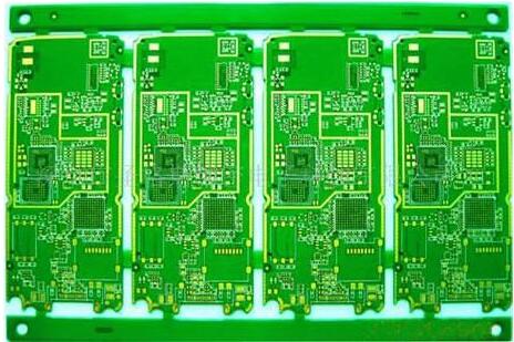
As smartphones, tablets, and other mobile electronic devices continue to become smaller, thinner, lighter, and more portable, the available space inside their mainboards is becoming increasingly limited. At the same time, consumers expect these devices to provide more functions and higher performance.
This trend has increased demand for HDI PCB technology.
Compared with conventional multilayer boards, HDI technology uses microvias, blind vias, buried vias, and high-density routing structures to make more efficient use of limited board space. By reducing unnecessary through-hole structures and shortening interconnection paths, an HDI Circuit Board can accommodate more components within a smaller footprint.
As a result, HDI technology has become an important solution for compact, high-performance electronic products.
Why HDI PCB Is Important for Mobile Devices
The continuous development of smartphones and tablets requires increasingly sophisticated PCB structures.
Modern mobile devices integrate processors, memory, power-management circuits, RF modules, cameras, sensors, wireless communication systems, and other components into an extremely limited space.
Traditional multilayer PCBs may not provide sufficient routing density for some of these designs.
An HDI PCB addresses this challenge by using advanced interconnection structures, including:
- Microvias
- Blind vias
- Buried vias
- Fine-line routing
- Fine-pitch component connections
- Sequential build-up structures
- High-density component placement
These technologies allow designers to route more signals without simply increasing the overall board size.
The result is a smaller and more efficient PCB structure that supports the miniaturization of modern mobile electronics.
HDI Technology Enables Higher Routing Density
One of the major advantages of High-Density PCB technology is its ability to increase routing density.
In a conventional multilayer PCB, through-holes may occupy routing space across multiple layers. By using blind and buried vias, HDI structures can provide more flexibility for layer-to-layer connections.
Microvias are particularly useful for fine-pitch components because their smaller dimensions allow routing channels to be placed more efficiently around component pads.
However, increasing density also introduces additional manufacturing challenges. PCB designers and manufacturers must carefully control:
- Line width and spacing
- Microvia diameter
- Via-to-pad registration
- Layer-to-layer alignment
- Copper thickness
- Dielectric thickness
- Via reliability
- Impedance requirements
Therefore, high-density design must be developed together with realistic manufacturing capabilities.
The Development of Any-Layer HDI
As mobile devices continue to evolve, HDI structures have progressed from relatively simple first-order configurations toward more advanced sequential-build-up and any-layer HDI structures.
Any-layer HDI allows microvias to be formed between adjacent layers, providing greater freedom for interconnection and routing.
This structure can help designers optimize:
- Component placement
- Signal routing
- Power distribution
- Ground connections
- Board thickness
- Routing density
The exact HDI structure required depends on the product’s electrical performance, component density, mechanical dimensions, reliability requirements, and manufacturing capability.
For high-end smartphones and compact computing devices, advanced HDI technology can provide significant advantages in reducing PCB size while maintaining complex electrical functionality.
HDI PCB Drives Growth in the Mobile Electronics Market
The continued expansion of smartphones, tablets, wearable electronics, and other portable devices has created sustained demand for advanced PCB technologies.
As product functions increase, the PCB must support more connections while maintaining a small form factor.
This creates a direct relationship between product miniaturization and PCB technology development.
The adoption of HDI PCB technology allows manufacturers to increase interconnection density without relying solely on additional board layers or a larger board footprint.
For this reason, mobile electronics have become one of the important application areas for HDI manufacturing.
High-End Servers Also Increase Demand for HDI
Mobile devices are not the only products driving demand for high-density PCB technology.
High-performance servers, networking equipment, data-center systems, and other advanced computing platforms also require increasingly sophisticated PCB structures.
Entry-level electronic products may use relatively simple PCB constructions, while high-performance computing equipment often requires significantly more layers and more complex routing.
High-end server motherboards may use large multilayer structures with many signal, power, and ground layers. Some advanced systems can also incorporate HDI structures to improve routing density and support high-speed interconnections.
The requirements are especially demanding for systems containing multiple processors, high-speed memory, networking interfaces, storage interfaces, and high-current power-delivery networks.
HDI in High-Performance Server Applications
A server PCB must simultaneously handle high-speed signals, high power density, thermal management, and complex interconnect structures.
The PCB design may need to accommodate:
- High-speed differential signals
- High-speed memory interfaces
- Multiple processors
- High-density connectors
- Power distribution networks
- High-current power delivery
- High-speed networking interfaces
- Complex grounding structures
In these applications, Multilayer PCB technology provides the necessary layer count, while HDI structures can further improve routing flexibility in areas with extremely high component density.
However, HDI should not automatically be applied to every server design. The appropriate PCB structure should be selected according to electrical requirements, routing complexity, mechanical constraints, cost targets, and manufacturing capability.
Cloud Computing Creates Additional PCB Demand
The rapid development of cloud computing and data-center infrastructure has increased demand for high-performance servers and networking equipment.
Cloud platforms support applications such as:
- Online services
- Digital payments
- Social networking
- Artificial intelligence
- Big-data processing
- Enterprise applications
- Video streaming
- Cloud storage
As these services expand, data centers require greater computing and networking capacity.
Higher processing performance generally means more complex hardware architectures, which in turn increase requirements for PCB layer structures, signal integrity, power integrity, thermal management, and manufacturing precision.
This creates additional opportunities for advanced HDI Circuit Board technology in the server and networking markets.
HDI PCB Design Challenges
Although HDI provides significant advantages in terms of density, its design and manufacturing requirements are more demanding than those of conventional PCBs.
Microvia Reliability
Microvias are smaller than conventional through-holes and must be designed carefully to ensure sufficient reliability.
Parameters such as microvia diameter, depth, aspect ratio, copper plating quality, pad geometry, and stacking structure can affect reliability.
Registration Accuracy
As the number of build-up layers increases, layer-to-layer registration becomes increasingly important.
Small alignment errors can affect via connections, fine-pitch pads, trace spacing, and overall manufacturability.
Signal Integrity
High-density routing often places high-speed signals close together.
Designers therefore need to consider:
- Controlled impedance
- Crosstalk
- Return-current paths
- Via transitions
- Reference planes
- Differential-pair routing
- Signal loss
For high-speed server and mobile applications, HDI PCB design must balance routing density with electrical performance.
Thermal Management
Higher component density can also increase localized heat generation.
The PCB structure should therefore be evaluated together with component placement, copper distribution, thermal vias, power delivery, and the system-level cooling strategy.
PCB Manufacturing Requirements for HDI
Advanced PCB Manufacturing capabilities are essential for producing reliable HDI boards.
Key manufacturing processes may include:
- Inner-layer circuit fabrication
- Sequential lamination
- Laser microvia drilling
- Desmear and hole preparation
- Electroless copper deposition
- Electroplated copper
- Fine-line pattern formation
- Layer registration control
- Surface finishing
- Electrical testing and reliability inspection
Each stage requires tight process control.
The manufacturer’s capabilities should be evaluated before finalizing the HDI design. Design rules should reflect actual production capabilities rather than theoretical minimum dimensions.
HDI PCB and Conventional Multilayer PCB
HDI and conventional multilayer boards each have their own suitable applications.
A conventional Multilayer PCB may be sufficient when the product has moderate routing density, larger components, and less demanding mechanical constraints.
HDI becomes more attractive when the design requires:
- Smaller board dimensions
- Higher routing density
- Fine-pitch components
- More compact interconnections
- Advanced miniaturization
- Complex component placement
The decision should therefore be based on the complete electrical, mechanical, manufacturing, and cost requirements of the product.
Kingda’s HDI PCB Manufacturing Capabilities
At Kingda, HDI production is supported by a manufacturing approach that combines PCB design considerations, material selection, process engineering, and quality control.
For mobile electronics, computing systems, networking equipment, and other high-density applications, the appropriate HDI structure can be evaluated according to:
- Layer count
- Line width and spacing
- Microvia structure
- Board thickness
- Material selection
- Controlled impedance requirements
- Component density
- Reliability requirements
- Production volume
Early communication between the PCB designer and manufacturer is especially important for advanced HDI projects.
A design that considers manufacturability from the beginning can help reduce unnecessary redesigns, improve yield, and achieve more stable production.
The Future of HDI PCB Technology
The continued development of mobile devices, cloud computing, data centers, artificial intelligence, networking, and other high-performance applications will continue to increase demand for high-density interconnection technologies.
Future PCB development is expected to focus on:
- Higher routing density
- Smaller microvias
- Finer line widths and spacing
- Improved registration accuracy
- Better high-speed signal performance
- Higher layer-count structures
- Improved thermal management
- Greater manufacturing reliability
At the same time, advanced HDI manufacturing must balance miniaturization with cost, yield, reliability, and production capability.
Conclusion
The development of smartphones and tablets has significantly increased demand for HDI PCB technology because manufacturers need to integrate more functions into increasingly compact products.
At the same time, high-performance servers, cloud computing infrastructure, networking equipment, and data centers are creating additional demand for high-density and advanced multilayer PCB structures.
By combining microvias, blind vias, buried vias, fine-line routing, and sequential build-up technology, an HDI Circuit Board can provide greater routing flexibility within a limited space.
However, successful HDI production depends not only on design density but also on registration accuracy, material selection, signal integrity, thermal management, microvia reliability, and manufacturing process control.
For advanced electronic products, selecting the right PCB structure and working with an experienced PCB Manufacturing partner are essential steps toward achieving reliable, high-density circuit board production.