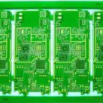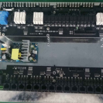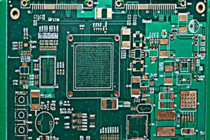
As electronic products continue to become smaller, faster, and more functionally integrated, printed circuit boards are evolving from simple single-sided and double-sided structures toward increasingly sophisticated multilayer configurations.
A Multilayer PCB can accommodate a large number of signal, power, and ground connections within a relatively compact board structure. However, as layer counts increase and line widths become finer, the requirements for manufacturing precision and reliability also become more demanding.
Among all manufacturing stages, Multilayer PCB Lamination is one of the most critical processes.
Lamination determines how the inner-layer circuits, dielectric materials, and copper foils are bonded into a unified PCB structure. Problems during lamination can result in layer misalignment, resin voids, delamination, board warpage, insufficient dielectric thickness, and other reliability issues.
Therefore, controlling the PCB Lamination Process requires coordinated management of material selection, inner-layer preparation, stackup design, temperature, pressure, heating rate, and curing conditions.
1. Design the Inner Core to Meet Lamination Requirements
Modern lamination equipment increasingly uses vacuum-assisted or vacuum lamination technology to reduce trapped air and improve resin filling.
Because lamination takes place within a controlled and relatively closed environment, the inner core must be properly designed and prepared before entering the press.
Several factors should be considered.
Core Thickness Selection
The thickness of the inner core should be selected according to the total thickness and electrical requirements of the finished Multilayer PCB.
For multilayer boards, especially higher-layer-count designs, consistent core thickness is important for maintaining the intended stackup and dielectric structure.
Core materials should have stable dimensional characteristics, and the material orientation should be considered when assembling the stackup.
Improper material orientation or unbalanced construction can contribute to PCB warpage after lamination.
Keep Sufficient Panel Clearance
The effective circuit area should maintain an appropriate distance from the panel edge.
This clearance provides sufficient space for:
- Tooling holes
- Registration features
- Mechanical processing
- Routing or profiling
- Lamination support
- Manufacturing tolerances
As the layer count and board complexity increase, the required manufacturing margin may also need to increase.
The exact clearance should be determined according to the PCB manufacturer’s panelization and tooling requirements rather than applying a single universal value.
Design Accurate Registration Features
Layer-to-layer registration is critical in the PCB Lamination Process.
Misalignment between inner layers can affect:
- Via-to-pad registration
- Fine-pitch features
- Trace spacing
- Impedance structures
- Copper distribution
- Overall PCB reliability
Production panels may therefore use tooling holes, registration targets, rivet holes, and other alignment features.
For high-layer-count boards, more sophisticated registration systems may be required to maintain alignment throughout multiple lamination cycles.
The specific tooling structure depends on the manufacturer’s equipment, panel design, and PCB construction.
Keep the Inner Core Clean and Defect-Free
Before lamination, the inner core should be inspected to ensure that it is free from:
- Open circuits
- Shorts
- Foreign particles
- Residual photoresist
- Excessive oxidation
- Surface contamination
- Other visible defects
A contaminated or defective inner layer can become permanently encapsulated during lamination, making subsequent repair extremely difficult or impossible.
2. Select the Appropriate Prepreg and Copper Foil
Material selection is another important factor in Multilayer PCB Lamination.
Prepreg, commonly abbreviated as PP, serves as the dielectric bonding material between PCB layers.
During lamination, the resin in the prepreg softens, flows, fills appropriate surface features, and then cures to form a solid dielectric layer.
The selection of prepreg should consider the required:
- Dielectric thickness
- Dielectric constant (Dk)
- Dissipation factor (Df)
- Controlled impedance
- Electrical strength
- Resin content
- Mechanical strength
- Thermal performance
- Lamination compatibility
Prepreg Resin Flow
One of the primary functions of prepreg is to provide sufficient resin flow during lamination.
The resin must be capable of filling appropriate spaces between copper features while producing a stable dielectric structure after curing.
Insufficient resin flow can result in voids or incomplete filling.
Excessive resin flow, however, can cause resin squeeze-out, changes in dielectric thickness, or movement of circuit features.
Therefore, prepreg selection should be based on the actual copper pattern, layer structure, thickness requirements, and lamination process.
Dielectric Thickness
The prepreg combination determines a significant portion of the final dielectric thickness between conductive layers.
For impedance-controlled designs, dielectric thickness is particularly important because it affects transmission-line geometry and impedance.
The final dielectric thickness should therefore be evaluated after considering resin content, copper thickness, copper pattern density, press conditions, and resin flow.
Symmetrical Stackup Design
A balanced PCB Stackup is important for controlling board warpage and maintaining mechanical stability.
For example, copper distribution, dielectric thickness, and material structures should be evaluated across the center of the stackup.
An unbalanced stackup can create uneven mechanical stress during heating and cooling, increasing the risk of bow and twist.
Copper Foil Selection
Copper foil should be selected according to the electrical, thermal, mechanical, and manufacturing requirements of the PCB.
Important parameters include:
- Copper thickness
- Surface profile
- Tensile strength
- Elongation
- Surface treatment
- High-frequency performance requirements
The selected copper foil should also be compatible with the intended PCB fabrication and lamination process.
3. Inner-Layer Surface Treatment
Before lamination, inner-layer copper surfaces normally require appropriate surface treatment.
Traditional processes may include oxide treatment, while modern production can also use alternative oxide or oxide-replacement treatments depending on the manufacturing system.
The purpose is not simply to change the copper color. The treatment modifies the copper surface to improve bonding with the resin system.
Main Functions of Inner-Layer Treatment
A properly controlled treatment can:
- Increase the effective surface area of the copper.
- Improve resin wetting.
- Increase adhesion between copper and dielectric material.
- Improve resistance to thermal stress.
- Reduce the risk of interfacial separation.
During lamination, molten resin must adequately wet the treated copper surface and form a reliable interface after curing.
The surface condition should therefore be controlled carefully.
Excessive treatment can also be undesirable because it may affect copper surface characteristics and dimensional stability.
4. Control the PCB Lamination Parameters
The major parameters in the PCB Lamination Process include:
- Temperature
- Pressure
- Time
- Heating rate
- Vacuum conditions
- Resin flow
- Cooling rate
These parameters are interrelated and should be optimized according to the specific resin system, prepreg construction, copper pattern, layer count, and board thickness.
Temperature Control
Temperature is one of the most important lamination parameters.
During heating, the resin typically passes through several stages:
Softening → Melting and Flow → Wetting and Filling → Gelation → Curing
As the temperature increases, the prepreg resin becomes increasingly fluid and begins to flow.
This flow allows the resin to fill appropriate spaces and wet the copper surfaces.
As curing progresses, the resin viscosity increases until the material becomes a solid, cross-linked dielectric.
The exact temperature points depend on the resin system and prepreg specification. Therefore, manufacturers should use the recommended lamination profile provided for the selected material rather than relying on a fixed temperature for every PCB.
Heating Rate
The heating rate is another important parameter in Lamination Quality.
If the board heats too quickly, the resin may not have enough time to flow and wet the copper surface properly before significant curing occurs.
This can affect:
- Resin filling
- Interlayer bonding
- Void formation
- Dielectric uniformity
- Board warpage
If the heating rate is too slow, production efficiency may decrease and the resin may experience an inappropriate thermal history.
For this reason, heating profiles should be developed according to the prepreg system and validated through actual production.
The original process reference mentions heating rates around 1.5–4°C/min depending on the PP construction. Such values should be treated as process references rather than universal requirements.
5. Pressure and Vacuum Control
Pressure is applied during lamination to consolidate the stackup and help the resin fill appropriate areas.
Vacuum assistance can help remove trapped air and volatile materials from the laminate structure.
Proper pressure and vacuum control can improve:
- Interlayer bonding
- Resin filling
- Surface flatness
- Void control
- Laminate density
- Overall Lamination Quality
However, excessive pressure can also cause excessive resin squeeze-out or changes in the intended dielectric structure.
Therefore, pressure should be matched to the resin system, stackup, copper pattern, and board construction.
6. Cooling After Lamination
Cooling is an often-overlooked part of the PCB Lamination Process.
After the resin has sufficiently cured, the laminated panel must be cooled under controlled conditions.
Rapid or uneven cooling can generate thermal stress because different materials have different coefficients of thermal expansion.
Controlled cooling can help reduce:
- Board warpage
- Bow and twist
- Internal stress
- Dimensional instability
For high-layer-count boards, maintaining a stable and symmetrical construction throughout the heating and cooling cycle is particularly important.
7. Common Multilayer PCB Lamination Problems
Poor lamination control can lead to several manufacturing defects.
Delamination
Delamination refers to separation between material interfaces within the PCB structure.
Potential causes include:
- Poor copper surface preparation
- Insufficient resin bonding
- Moisture
- Contamination
- Incorrect lamination profile
- Inadequate curing
Resin Voids
Voids can occur when air or volatile materials remain trapped within the laminate.
Insufficient vacuum, inappropriate resin flow, contamination, or improper process parameters may contribute to this problem.
Board Warpage
Board warpage can result from:
- Unbalanced copper distribution
- Asymmetrical stackup
- Uneven resin distribution
- Material mismatch
- Uneven heating or cooling
- Internal thermal stress
A symmetrical PCB Stackup and properly controlled lamination profile can help reduce these risks.
Layer Misregistration
Layer misalignment becomes increasingly important as line widths and spacing become smaller.
Poor tooling, material movement, thermal expansion, or insufficient registration compensation can affect layer alignment.
For advanced multilayer boards, registration should be monitored throughout the manufacturing process.
8. Lamination Quality Inspection
After lamination, manufacturers should verify whether the laminated structure meets design and manufacturing requirements.
Depending on the PCB type, inspection may include:
- Visual inspection
- Thickness measurement
- Dimensional inspection
- Layer registration inspection
- Cross-sectional analysis
- Microsection analysis
- Bonding evaluation
- Thermal reliability testing
- Electrical testing
For high-reliability applications, additional testing may be required to evaluate resistance to thermal cycling, moisture, soldering temperatures, and mechanical stress.
9. Design for Manufacturability in Multilayer PCB Lamination
Lamination quality does not depend solely on the pressing process.
Good PCB Manufacturing results begin during PCB design.
Designers should consider:
- Symmetrical stackup construction
- Copper balance
- Material compatibility
- Dielectric thickness
- Impedance requirements
- Registration tolerances
- Via structures
- Board thickness
- Thermal expansion
- Manufacturing capability
For example, a theoretical stackup may appear acceptable in a PCB design tool but may be difficult to manufacture consistently if it requires extremely tight registration or unusual prepreg combinations.
Early DFM communication between the designer and PCB manufacturer can significantly improve production stability.
10. Kingda’s Multilayer PCB Lamination Approach
At Kingda, multilayer board production combines stackup engineering, material selection, inner-layer preparation, lamination process control, and quality inspection.
For different Multilayer PCB structures, the lamination process can be evaluated according to:
- Layer count
- Finished board thickness
- Copper thickness
- Prepreg construction
- Dielectric requirements
- Impedance requirements
- Copper distribution
- Registration requirements
- Reliability standards
- Production volume
The goal is to ensure that the selected materials and lamination profile are compatible with the actual PCB structure.
For advanced multilayer designs, process engineering at the early design stage can help reduce registration problems, warpage, bonding defects, and unnecessary production adjustments.
Conclusion
Multilayer PCB Lamination is a fundamental process for producing reliable high-layer-count circuit boards.
Achieving stable Lamination Quality requires more than simply controlling press temperature. Core thickness, stackup symmetry, registration design, prepreg selection, copper foil, inner-layer surface treatment, resin flow, pressure, vacuum, heating rate, curing, and cooling must all work together.
As PCB technology moves toward higher density, finer features, thinner dielectric structures, and more complex electrical requirements, the PCB Lamination Process must become increasingly precise and consistent.
By combining manufacturable PCB Stackup design with appropriate materials and controlled PCB Manufacturing processes, manufacturers such as Kingda can support the production of reliable multilayer PCBs for demanding electronic applications.