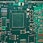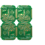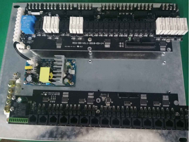
The development of the Printed Circuit Board (PCB) fundamentally changed the electronics industry. Before the invention of the PCB, electronic components were primarily interconnected using point-to-point wiring. As electronic products became smaller, more complex, and more reliable, traditional wiring methods could no longer meet the requirements of mass production.
The development of modern PCB technology provided a more compact, reliable, and repeatable method for connecting electronic components. Today, PCBs are essential components in almost every electronic product, ranging from consumer electronics and computers to automotive electronics, industrial equipment, telecommunications systems, and aerospace applications.
The History of PCB Development
In 1936, Austrian engineer Paul Eisler developed and patented an early form of printed circuit technology and applied the concept to radio equipment. His work demonstrated that conductive patterns could be used to replace a large amount of conventional point-to-point wiring.
During the 1940s, printed circuit technology attracted increasing attention, particularly for military and communication equipment. By 1948, the technology had been approved for commercial applications in the United States. From the mid-1950s onward, Printed Circuit Boards began to see much broader adoption as electronic manufacturing developed rapidly.
Before the widespread use of PCBs, electronic components were connected with individual wires. This approach required considerable manual assembly and made complex circuits difficult to manufacture consistently. As circuit density increased, point-to-point wiring became increasingly impractical.
The introduction of the Printed Circuit Board solved many of these problems by integrating conductive traces, pads, and other circuit features onto a rigid or flexible substrate. This enabled manufacturers to produce electronic circuits with greater consistency, repeatability, and assembly efficiency.
Why Multilayer PCBs Were Developed
As electronic systems became more sophisticated, designers needed more routing space without continuously increasing the physical size of the board. This requirement led to the development of multilayer circuit structures.
A Multilayer PCB is constructed by combining multiple conductive layers with insulating dielectric materials. Depending on the design, the stackup may include signal layers, power planes, ground planes, and additional routing layers.
For example, a four-layer PCB may typically contain:
- A top signal layer
- An inner ground or power plane
- An inner power or ground plane
- A bottom signal layer
A six-layer design can provide additional signal and plane layers, offering greater routing density and improved power distribution.
The conductive layers are interconnected using plated through-holes, blind vias, buried vias, and other interconnection structures. This approach allows designers to achieve higher circuit density while maintaining a manageable board size.
Copper Clad Laminate: The Foundation of PCB Manufacturing
Copper clad laminate (CCL) is one of the fundamental materials used in PCB Manufacturing. It consists of an insulating substrate reinforced with materials such as fiberglass and resin, with copper foil bonded to one or both sides.
CCL provides both mechanical support and electrical functionality. The copper layer can be patterned to create traces, pads, planes, and other conductive structures, while the dielectric material provides electrical insulation between conductive layers.
During the early development of PCB technology, researchers explored different combinations of resins, reinforcing materials, and insulating substrates. These developments eventually created the material foundation required for modern PCB production.
At the same time, subtractive circuit manufacturing based on copper foil patterning and etching became an important production method. This manufacturing approach strongly influenced the structure, material requirements, and performance characteristics of copper clad laminates.
Modern CCL materials are available in many grades to meet different requirements, including:
- Standard FR-4 materials
- High-Tg materials
- Low-loss materials
- High-frequency materials
- Halogen-free materials
- Flexible circuit materials
- High-speed digital materials
Material selection depends on electrical performance, thermal requirements, mechanical reliability, operating environment, and manufacturing requirements.
PCB Lamination Process
For a multilayer board, PCB Lamination is a critical manufacturing step. Lamination combines inner-layer cores, prepreg, and copper foil under controlled temperature, pressure, and vacuum conditions to form a solid multilayer structure.
For example, a typical four-layer PCB may use:
- One inner-layer core
- Two sheets or e outer layers
The actual material configuration depends on the required stackup, dielectric thickness, copper thickness, impedance requirements, and material system.
During PCB Lamination, the resin in the prepreg softens and flows under heat and pressure. It fills the required spaces between conductive layers and bonds the individual materials together. The resin then cures to form a stable multilayer structure.
Proper lamination control is essential because excessive resin flow, insufficient bonding, trapped air, layer misregistration, or uneven pressure can affect PCB reliability.
Important lamination parameters include:
- Temperature profile
- Heating rate
- Pressure
- Vacuum
- Resin flow
- Curing time
- Cooling rate
- Stackup symmetry
The specific lamination recipe should be established according to the material manufacturer’s specifications and the PCB manufacturer’s process capability rather than applying a single universal temperature or pressure value.
PCB Drilling Process
Drilling is another essential stage in PCB Manufacturing. Different types of holes may be required depending on the electrical and mechanical functions of the board.
For conventional multilayer PCBs, plated through-holes are drilled through the entire board thickness. After drilling, the hole walls are chemically treated and plated with copper so that electrical connections can be established between conductive layers.
These plated holes can be used for:
- Through-hole component leads
- Layer-to-layer electrical connections
- Via structures
- Ground connections
- Power connections
Not every hole on a PCB requires copper plating. Mechanical holes, mounting holes, tooling holes, and certain thermal or structural holes may be designed as non-plated holes when electrical connectivity is not required.
Modern high-density boards may also use laser-drilled microvias and other advanced interconnection structures. These technologies are particularly important for HDI designs, where conventional through-hole structures may consume too much routing space.
PCB Imaging and Circuit Pattern Formation
Circuit patterns must be accurately transferred onto the copper surface during PCB production.
In a conventional imaging process, the copper surface is prepared with a photosensitive material. A circuit image is then transferred using an exposure system. Ultraviolet light selectively exposes the photosensitive layer according to the circuit pattern.
After development, the required circuit pattern is revealed and subsequent etching or plating processes can be performed.
Modern PCB manufacturers increasingly use laser direct imaging (LDI) and other digital imaging technologies to improve registration accuracy and support finer circuit features.
Accurate imaging is particularly important for high-density Multilayer PCB production because even small registration errors can affect line spacing, pad alignment, via connections, and overall board reliability.
Solder Mask: Protecting the PCB Surface
Solder Mask is the protective coating applied over selected areas of the PCB surface. It is commonly associated with the green coating seen on conventional circuit boards, although many other colors are available.
The primary functions of Solder Mask include:
- Preventing accidental solder bridging
- Protecting exposed copper from oxidation
- Reducing the risk of electrical shorts
- Improving insulation between adjacent conductors
- Protecting circuit features from environmental contamination
- Improving the overall durability of the PCB surface
The solder mask generally covers most exposed copper areas while leaving solder pads, test points, and other designated areas accessible.
Although green is the most common solder mask color, manufacturers can also provide black, blue, red, yellow, white, and other colors depending on application requirements.
Solder mask thickness, registration accuracy, opening dimensions, surface condition, and curing quality must be controlled carefully during production.
PCB Layers in Computer Motherboards
Computer motherboards are a typical example of how multilayer circuit technology is used in complex electronic systems.
Depending on the product class and design requirements, a motherboard may use four, six, eight, or even more PCB layers.
A basic four-layer structure may include:
- Top signal layer
- Ground plane
- Power plane
- Bottom signal layer
A six-layer board may introduce additional signal and reference layers to provide more routing space and better control of power and signal distribution.
Increasing the number of PCB layers does not automatically guarantee better electromagnetic performance. However, a properly designed multilayer stackup can provide advantages such as:
- Improved signal integrity
- Better power distribution
- More continuous return-current paths
- Better electromagnetic compatibility (EMC)
- Higher routing density
- Improved control of controlled-impedance traces
- Better separation between sensitive and noisy circuits
For high-speed motherboards, stackup design must consider signal integrity, power integrity, impedance control, return paths, crosstalk, via transitions, and manufacturing tolerances.
The Importance of PCB Manufacturing Technology
Modern PCB Manufacturing is no longer limited to simple copper etching. Advanced production may involve precision imaging, laser drilling, microvia formation, sequential lamination, fine-line processing, surface finishing, automated optical inspection, electrical testing, and other specialized technologies.
As electronic products continue to become smaller and more powerful, PCB manufacturers must achieve increasingly demanding requirements for:
- Fine line and spacing
- Small via structures
- High layer counts
- Tight layer-to-layer registration
- Controlled impedance
- High-density interconnects
- Thermal reliability
- Mechanical reliability
- Surface quality
- Manufacturing consistency
For this reason, PCB design and manufacturing should be considered together. A design that appears electrically feasible may still require modification if it exceeds the manufacturer’s actual process capability.
Kingda’s Approach to PCB Manufacturing
At Kingda, PCB development and production can be evaluated from both design and manufacturing perspectives. For multilayer and high-density circuit boards, factors such as stackup configuration, material selection, lamination, drilling, imaging, plating, solder mask, surface treatment, and electrical testing all contribute to final product quality.
A reliable manufacturing process should not only meet the nominal dimensions specified in PCB design files but also maintain stable process control throughout production.
By combining appropriate material selection, manufacturing capability, process control, and quality inspection, Kingda supports the production of PCBs for a wide range of electronic applications.
Conclusion
The history of the Printed Circuit Board reflects the continuous evolution of electronic technology. From early printed circuit concepts developed for radio equipment to today’s sophisticated Multilayer PCB structures, PCB technology has enabled electronic products to become smaller, faster, more reliable, and more functional.
The modern PCB Manufacturing process integrates material engineering, circuit imaging, etching and plating, PCB Drilling, PCB Lamination, solder mask application, surface finishing, and comprehensive inspection.
As electronic systems continue to demand higher density, faster signal speeds, greater reliability, and smaller form factors, PCB technology will continue to evolve. Advanced materials, HDI structures, fine-line circuits, sequential lamination, and high-precision manufacturing will play an increasingly important role in next-generation electronics.
For manufacturers and designers alike, understanding PCB materials, layer structures, manufacturing processes, and quality-control requirements is essential for developing reliable and cost-effective electronic products.