A successful electronic product requires more than a correct schematic and functional PCB layout. The design must also consider assembly processes, component tolerances, inspection requirements, testing accessibility, repairability, and high-volume production.
This is especially important for SMT Assembly, where fine-pitch components, high component density, small solder joints, and automated placement processes leave relatively little margin for manufacturing variation.
Designers should therefore consider manufacturing and assembly requirements from the beginning of the PCB Design process. A design that is difficult to assemble, inspect, or test may result in lower production yield, higher manufacturing costs, and more complicated rework.
For this reason, Design for Manufacturing (DFM) and Design for Assembly (DFA) should be integrated into the product development process rather than being treated as final-stage checks.
Process Planning for SMT Assembly
The first step is to establish a clear and repeatable Assembly Process.
A typical SMT production flow may include:
- PCB and component incoming inspection
- Solder paste printing
- Solder paste inspection (SPI)
- Automated component placement
- Pre-reflow inspection
- Reflow soldering
- Automated optical inspection (AOI)
- X-ray inspection where required
- Electrical testing
- Functional testing
- Final inspection and packaging
Each stage should have clearly defined process parameters and acceptance criteria.
For fine-pitch assemblies, continuous process monitoring is particularly important because small variations in solder paste volume, component placement, pad geometry, or reflow conditions can significantly affect solder-joint quality.
Applicable industry standards should also be identified during product development. For example, IPC standards such as IPC J-STD-001 and IPC-A-610 are commonly referenced for soldering process requirements and electronic assembly acceptance criteria. The exact standards should be selected according to the product, customer requirements, and applicable industry regulations.
Designing for High-Volume Production
A design intended for mass production should consider the entire transition from engineering prototype to stable production.
This includes:
- Assembly process requirements
- Component availability
- Manufacturing tolerances
- Automated placement
- Inspection
- Testing
- Repairability
- Reliability
- Production documentation
- Traceability
A complete manufacturing package is essential for consistent PCBA Manufacturing.
Essential Manufacturing Documentation
Depending on the project, the production package may include:
- Bill of Materials (BOM)
- Approved component or manufacturer information
- PCB fabrication drawings
- Assembly drawings
- Pick-and-place data
- Component X-Y coordinates
- Gerber or other fabrication data
- Drill files
- Assembly specifications
- Special process instructions
- Test-point information
- Electrical test requirements
- Inspection criteria
Clear documentation reduces communication errors between design, procurement, PCB fabrication, and assembly teams.
CAD Data and Assembly Tooling
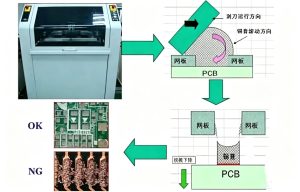
Accurate CAD and manufacturing data can be used to develop production tooling, inspection programs, and automated assembly equipment.
Important information may include:
- Component reference designators
- X-Y component coordinates
- Rotation angles
- Component side
- Polarity information
- Board outline
- Fiducial locations
- Test-point coordinates
- Keep-out areas
- Panelization information
Accurate data is particularly important for automated placement machines. Incorrect component coordinates or rotation information can result in misplaced or incorrectly oriented components.
For this reason, the assembly data should be verified before releasing the design to production.
PCBA Quality Control
Reliable PCB Assembly requires inspection and process control at multiple stages rather than relying only on final visual inspection.
Incoming Inspection
Incoming inspection can verify PCB quality, component specifications, packaging, markings, moisture sensitivity, and other requirements.
For critical components, manufacturers may also verify lot information and traceability documentation.
Solder Paste Printing
Solder paste printing is one of the most important stages in SMT Assembly.
The quality of solder paste deposition depends on factors such as:
- Stencil design
- Stencil thickness
- Aperture geometry
- Solder paste properties
- Printing speed
- Squeegee pressure
- PCB support
- Separation behavior
- Environmental conditions
SPI can be used to measure solder paste volume, height, area, and positional offset before components are placed.
Early detection of printing problems can prevent large numbers of defective assemblies from progressing to later production stages.
Reflow Soldering
After component placement, the PCB passes through a reflow soldering process.
The reflow profile must be developed according to the solder paste alloy, PCB construction, component requirements, thermal mass, and equipment characteristics.
Important parameters include:
- Preheat
- Soak
- Ramp rate
- Peak temperature
- Time above liquidus
- Cooling rate
The objective is to achieve reliable solder joints without exceeding component or PCB thermal limitations.
Fine-Pitch Component Assembly
Fine-Pitch Components create additional challenges because the distance between adjacent terminals is significantly reduced.
Fine-pitch packages may include:
- SOIC
- QFP
- TQFP
- QFN
- BGA
- CSP
- Other high-density packages
As pitch decreases, solder-paste volume, stencil aperture design, pad geometry, placement accuracy, and inspection become increasingly important.
A component pitch of approximately 0.025 inch (0.635 mm) or below is often considered fine pitch in many assembly contexts, although definitions vary by package and industry.
Designers should not rely on a single generic pad dimension. Recommended land patterns should be developed according to the actual component package drawing, applicable IPC land-pattern guidance, assembly process, and manufacturer’s capabilities.
Fine-Pitch Pad Design
Pad geometry directly influences solder-joint formation.
When developing land patterns for fine-pitch devices, designers should consider:
- Component terminal dimensions
- Nominal pitch
- Component tolerances
- PCB fabrication tolerances
- Placement accuracy
- Stencil aperture design
- Solder-mask registration
- Solder-joint requirements
IPC-7351 is commonly referenced for land-pattern development for surface-mount components. However, the manufacturer’s package drawing and customer-specific requirements should also be considered.
In some applications, the optimized production land pattern may differ from a generic library footprint because the assembly process and component tolerances must be taken into account.
Component Orientation in SMT Assembly
Consistent component orientation can improve assembly efficiency and inspection.
Polarized components should have clearly defined orientation, including:
- Diodes
- LEDs
- Electrolytic capacitors
- Tantalum capacitors
- ICs
- Connectors
- Other polarity-sensitive components
The PCB assembly drawing and silkscreen should provide unambiguous polarity markings.
For automated SMT placement, component rotation can generally be programmed by the placement equipment. However, maintaining consistent orientation within the design library can simplify programming, inspection, troubleshooting, and operator verification.
For wave soldering, component orientation can be even more important because solder flow direction and component geometry can influence soldering performance.
Component Spacing and Accessibility
A highly automated placement machine can position components with excellent repeatability. However, component placement must also account for inspection, soldering, rework, and maintenance.
A tall component positioned immediately beside a fine-pitch device may obstruct:
- AOI inspection
- Manual visual inspection
- Rework tools
- Soldering equipment
- Component replacement
- Probe access
Therefore, component spacing should not be determined solely by whether the placement machine can physically place the components.
Height and Shadowing Effects
Tall components can create shadowing effects during wave soldering and may prevent solder from reaching adjacent low-profile components.
For wave-soldered assemblies, the designer should consider:
- Component height
- Solder-flow direction
- Pad orientation
- Component spacing
- Thermal shadowing
- Keep-out areas
Not every SMT component is suitable for direct wave-solder exposure. Component specifications and the selected soldering process must be verified before production.
Standardized Component Libraries
Using standardized components and verified footprints can improve design consistency.
A controlled PCB component library should include:
- Manufacturer part number
- Package type
- Recommended land pattern
- Component dimensions
- Polarity
- Height
- Assembly side
- Approved alternatives
- Lifecycle information
Designers should avoid assuming that components with the same package name are physically identical across manufacturers.
For example, different suppliers may use slightly different package dimensions, terminal geometries, body sizes, or tolerances even when the components are described using the same general package designation.
Therefore, the actual component datasheet should always be checked before finalizing the footprint.
Designing for Production Efficiency
A board can be electrically sophisticated without being unnecessarily difficult to manufacture.
Production efficiency can often be improved through thoughtful component placement and standardized design rules.
Key considerations include:
- Minimize unnecessary component variation
- Use consistent component orientations
- Standardize footprints
- Avoid unnecessary package types
- Maintain sufficient inspection access
- Optimize panel utilization
- Provide appropriate fiducials
- Consider automated test requirements
- Design for efficient rework
If a PCB is very small, irregularly shaped, or contains components close to the board edge, panelization should be evaluated carefully.
Depending on the board geometry and assembly process, a suitable panel design may use breakaway tabs, mouse bites, V-grooves, or other depanelization methods. The appropriate method depends on the PCB material, component placement, edge requirements, and assembly equipment.
Testability and PCBA Testing
Testability should be considered during the initial PCB Design stage.
A board that cannot be tested efficiently can create significant production and troubleshooting costs.
In-Circuit Testing
In-circuit testing (ICT) can be used to evaluate electrical characteristics and detect certain assembly faults.
Depending on the test strategy, the PCB may require accessible test points connected to important nets.
Test points should be:
- Electrically accessible
- Mechanically accessible
- Appropriately spaced
- Clearly documented
- Located where the fixture or probe can reach them
Not every product requires ICT. The appropriate test method depends on production volume, product complexity, fault coverage, cost, and customer requirements.
Functional Testing
Functional testing verifies whether the assembled product operates as intended.
It can evaluate:
- Power-up behavior
- Communication
- Sensors
- Displays
- Interfaces
- Control functions
- Output signals
- System-level performance
Functional testing is particularly valuable when certain internal connections cannot be fully evaluated through ICT or when the product’s system behavior must be verified.
Automated Optical Inspection
AOI is widely used in PCBA Manufacturing to detect visible assembly defects.
Depending on the equipment and program, AOI can identify problems such as:
- Missing components
- Incorrect component placement
- Incorrect orientation
- Solder bridging
- Insufficient visible solder
- Excess solder
- Component offset
- Polarity errors
However, AOI cannot inspect every type of solder joint. For hidden joints such as many BGA connections, X-ray inspection may be more appropriate.
X-Ray Inspection for Hidden Solder Joints
X-ray inspection can provide valuable information about solder joints that cannot be directly observed from the PCB surface.
It may be used for packages such as:
- BGA
- QFN with bottom termination
- Bottom-terminated components
- Other concealed solder connections
Depending on the equipment, X-ray inspection can help identify voiding, bridging, insufficient solder, and other internal defects.
The inspection criteria should be established according to the component type, soldering process, applicable standards, and customer requirements.
Repair and Rework Considerations
A production-ready design should also consider how defective components can be replaced.
Components positioned too closely together may make rework difficult even when the initial assembly process is successful.
Therefore, designers should provide adequate access around critical components and avoid unnecessary mechanical obstructions.
This is especially important for:
- Fine-pitch ICs
- BGA components
- High-value components
- Connectors
- Power devices
- Components subject to field replacement
A balance should be established between high component density and practical serviceability.
Improving PCBA Reliability
Reliability begins with design and continues throughout manufacturing.
Important factors include:
- Appropriate component selection
- Correct land-pattern design
- Controlled solder-paste deposition
- Stable component placement
- Proper reflow profiling
- Adequate PCB cleanliness
- Thermal management
- Mechanical support
- Electrical testing
- Process traceability
For demanding applications, reliability testing may include thermal cycling, vibration, humidity, mechanical testing, or other qualification procedures according to the product environment.
Kingda’s Approach to PCB Assembly
Kingda supports customers by connecting PCB Design, fabrication, assembly, inspection, and testing into an integrated manufacturing workflow.
During engineering review, potential production risks can be identified before the PCB enters mass production.
Areas of review may include:
- PCB manufacturability
- Component availability
- Footprint verification
- Stencil design
- Component spacing
- Assembly orientation
- Test-point accessibility
- Panelization
- Inspection requirements
- Production documentation
This integrated approach helps improve manufacturing consistency while reducing avoidable design changes and rework.
Conclusion
Successful SMT Assembly depends on much more than automated component placement. A production-ready PCB must be designed with manufacturing, inspection, testing, reliability, and repairability in mind.
By applying Design for Manufacturing, optimizing Fine-Pitch Components and their land patterns, maintaining appropriate component spacing, standardizing footprints, and planning PCBA Testing from the beginning, engineers can improve production yield and reduce manufacturing risks.
A well-structured Assembly Process, combined with effective inspection and testing, provides a strong foundation for reliable PCBA Manufacturing.
Kingda can work with customers throughout the PCB development and assembly process to help transform engineering designs into manufacturable, testable, and reliable electronic products.