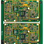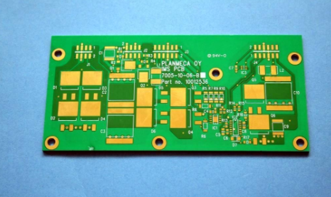
In LED lighting systems, the power supply and driver circuit directly affect efficiency, thermal performance, electromagnetic compatibility, and overall product reliability. A well-designed LED Driver PCB is therefore essential for converting and regulating electrical power while maintaining stable LED current and minimizing unwanted electromagnetic interference.
In addition to the schematic, the physical implementation of the board has a significant influence on electrical performance. A carefully planned PCB Layout can help reduce parasitic inductance, voltage overshoot, noise coupling, thermal problems, and manufacturing risks.
For this reason, LED Driver PCB Design should be considered as a combination of electrical design, component placement, routing, thermal management, EMI control, and manufacturability.
From Schematic to PCB Design
A typical PCB Design workflow for an LED driver or power supply can include the following stages:
- Create and verify the schematic.
- Generate the netlist and assign component footprints.
- Define board parameters and design rules.
- Establish the layer stackup and copper configuration.
- Place critical components.
- Route power and signal connections.
- Add grounding and copper planes where appropriate.
- Review thermal and EMI considerations.
- Perform design-rule checking (DRC).
- Complete engineering review.
- Generate manufacturing data for PCB Manufacturing.
Each stage can affect the final performance of the Power Supply PCB. A schematic may be electrically correct while the physical layout still creates excessive noise, voltage drops, thermal concentration, or difficult manufacturing conditions.
PCB Design Specifications for LED Driver Boards
The design rules for an LED Driver PCB should be established according to operating voltage, current, component characteristics, safety requirements, environmental conditions, and the manufacturer’s actual process capability.
Trace Spacing
The clearance between adjacent conductors must satisfy the applicable electrical safety and manufacturing requirements.
A larger clearance generally provides greater manufacturing margin, but excessive spacing can unnecessarily increase board size. Therefore, the appropriate value should be determined according to:
- Working voltage
- Transient voltage
- Creepage requirements
- Pollution degree
- Insulation system
- Manufacturing capability
- Applicable safety standards
For low-voltage signal circuits, spacing can often be optimized according to the manufacturer’s design rules. High-voltage sections require significantly more careful evaluation.
A fixed value such as 8 mil should not be treated as a universal requirement. The correct spacing depends on the application and the PCB manufacturer’s process capability.
Pad-to-Board-Edge Clearance
Adequate clearance should be maintained between copper pads, plated holes, and the PCB edge.
If a pad or plated hole is positioned too close to the board edge, mechanical routing, depanelization, plating, or assembly processes may create defects.
The actual minimum distance should therefore follow the board manufacturer’s fabrication capability and the selected edge-processing method.
Teardrop Connections
Where appropriate, a teardrop transition can be used between a trace and a pad or via.
The wider transition distributes mechanical and thermal stress more gradually and can improve manufacturing robustness, particularly when a relatively narrow trace connects to a larger pad or via.
However, teardrops are not required in every design. They should be applied according to the PCB manufacturer’s design rules and available space.
Component Placement Guidelines
Component placement is one of the most important parts of LED Driver PCB Design.
Even when the electrical schematic is correct, poor component placement can cause significant problems during operation.
For example, placing switching nodes, high-current loops, sensitive feedback traces, and control circuitry too close together can increase noise coupling.
A practical placement strategy should consider the functional blocks of the circuit.
Separate High-Current and Sensitive Circuits
Power components such as MOSFETs, inductors, diodes, transformers, and output capacitors should be positioned to minimize high-current loop area.
Sensitive components, including:
- Feedback resistors
- Current-sense circuits
- Controller ICs
- Reference circuits
- Communication interfaces
should be kept away from noisy switching nodes whenever possible.
This separation helps reduce unwanted coupling and improves the stability of the control loop.
Minimize Critical Current Loops
In a switching LED driver, rapidly changing currents flow through specific paths.
Large loop areas can increase parasitic inductance and electromagnetic radiation.
Therefore, the high-frequency switching loop should generally be kept as compact as practical. Connections between switching devices, diodes or synchronous rectifiers, inductors, and bypass capacitors should be carefully arranged.
This is particularly important for high-frequency power converters.
PCB Routing for LED Driver Circuits
Routing is another critical aspect of PCB Layout.
A PCB trace is not an ideal conductor. Its resistance, inductance, capacitance, geometry, and relationship with neighboring conductors can influence circuit behavior.
Power Trace Width
High-current traces should be designed according to the required current, allowable temperature rise, copper thickness, trace length, and available board area.
A wider trace generally reduces resistance and voltage drop, but simply making every power trace extremely wide is not always the best solution.
The designer should evaluate both electrical and thermal requirements.
For high-current LED driver outputs, particular attention should be paid to:
- Current density
- Copper thickness
- Trace width
- Temperature rise
- Connector capacity
- Via current distribution
- Thermal spreading
Keep High-Frequency Paths Short
Switching power supplies contain high-frequency current components. Long traces can increase parasitic inductance and create additional voltage spikes or EMI.
Critical switching paths should therefore be kept short and direct.
Avoid unnecessary:
- Long loops
- Sharp routing detours
- Excessive vias
- Large switching copper loops
- Uncontrolled return paths
A compact current loop is often one of the most effective ways to improve switching performance.
Grounding and Return-Current Paths
Grounding is a critical part of PCB Design, especially for switching LED drivers.
A poor grounding structure can allow high-current switching noise to interfere with feedback and control circuits.
Where practical, power ground and sensitive signal ground should be arranged so that high-current return currents do not unnecessarily flow through sensitive signal areas.
The grounding strategy depends on the specific circuit architecture. It may involve:
- Ground planes
- Star-point connections
- Kelvin sensing
- Dedicated return paths
- Local bypass capacitors
- Controlled current loops
The goal is to control where current flows rather than simply increasing the amount of copper.
EMI Control in LED Driver PCB Design
Switching LED drivers can generate electromagnetic interference because semiconductor devices rapidly switch voltage and current.
The main sources of EMI may include:
- High dv/dt switching nodes
- High di/dt current loops
- Transformer coupling
- Inductor radiation
- Long PCB traces
- Poor return-current paths
- Excessive parasitic inductance
Therefore, EMI Control should be considered from the beginning of the LED Driver PCB Design process.
Reduce Switching Loop Area
The area enclosed by rapidly changing current paths should be minimized.
A smaller loop generally reduces magnetic-field radiation and parasitic inductance.
Keep Noisy Nodes Away from Sensitive Traces
Switching nodes should be separated from:
- Feedback traces
- Current-sense traces
- Analog reference lines
- Communication signals
- LED control signals
Sensitive traces should also avoid running parallel to high-noise power traces for long distances.
Use Grounded Copper Carefully
Ground planes and copper areas can provide useful return paths and shielding when properly implemented.
However, simply filling every available area with copper does not automatically improve EMI performance. Copper geometry, current flow, layer structure, and reference-plane continuity must be considered together.
Decoupling Capacitor Placement
Decoupling capacitors should be placed close to the power pins of the relevant ICs or switching devices.
The connection between the capacitor and the device should be as short and low-inductance as practical.
Poor capacitor placement can significantly reduce the effectiveness of the capacitor at high frequencies.
For an LED Driver PCB, designers should consider both:
- Bulk capacitors for low-frequency energy storage
- High-frequency ceramic capacitors for local transient current
The appropriate capacitor combination depends on the converter topology, switching frequency, load conditions, and controller requirements.
Thermal Management
LED driver circuits can generate considerable heat, particularly in power semiconductors, inductors, transformers, resistors, and other power components.
Thermal design should therefore be integrated into the PCB Layout rather than being addressed after the board is completed.
Possible thermal management techniques include:
- Increasing copper area
- Using thermal vias
- Connecting thermal pads to internal or bottom copper
- Improving component spacing
- Providing adequate airflow
- Using external heat sinks where necessary
- Selecting components with appropriate thermal ratings
Thermal vias can help transfer heat from exposed pads to other copper layers, but their design should consider soldering requirements and manufacturing capability.
High-Speed Signals on LED Driver PCBs
Although an LED driver is primarily a power circuit, many modern systems also contain digital control, communication, PWM dimming, sensing, or monitoring functions.
These signals may require High-Speed PCB design practices when edge rates are sufficiently fast.
Important considerations include:
- Signal-return paths
- Trace impedance
- Trace length
- Crosstalk
- Reference-plane continuity
- Via transitions
- Ground separation
- Switching-noise coupling
A signal that appears to be “low frequency” based on its repetition rate can still contain high-frequency components because of its fast rise and fall times.
Therefore, signal integrity should be evaluated according to edge rate and interconnect behavior rather than frequency alone.
PCB Design Verification and DRC
After completing the PCB Layout, the design should undergo a detailed engineering review.
The review should verify both electrical requirements and manufacturing constraints.
Important checks include:
- Trace-to-trace clearance
- Trace-to-pad clearance
- Trace-to-via clearance
- Pad-to-via clearance
- Via-to-via spacing
- Copper-to-board-edge clearance
- High-voltage creepage and clearance
- Power trace width
- Grounding structure
- Thermal copper areas
- Component spacing
- Silkscreen placement
- Solder-mask openings
- Board outline
- Mounting-hole clearance
Design-rule checking should be performed before manufacturing data is released.
However, DRC alone cannot identify every potential problem. Engineering review is still necessary for thermal performance, current loops, EMI, component accessibility, and system-level reliability.
PCB Manufacturing Considerations
A good design must also be manufacturable.
The design rules used during PCB Design should be consistent with the capabilities of the selected PCB manufacturer.
Key manufacturing considerations include:
- Minimum trace width and spacing
- Copper thickness
- Hole size
- Aspect ratio
- Via structure
- Solder-mask registration
- Surface finish
- Board thickness
- Warpage control
- Panelization
- Electrical testing
Kingda can support customers by reviewing PCB designs from a manufacturing perspective and identifying potential risks before production.
This design-for-manufacturing approach can reduce unnecessary revisions, improve production yield, and help maintain consistent quality.
PCB Design Review Checklist
Before releasing an LED driver board for production, engineers can use a structured checklist covering the following areas:
Electrical Design
- Are voltage and current ratings appropriate?
- Are high-current paths sufficiently robust?
- Are creepage and clearance requirements satisfied?
- Are sensitive feedback circuits protected from switching noise?
Component Placement
- Are power components placed close to each other where required?
- Is the switching loop minimized?
- Are sensitive components separated from noisy nodes?
- Are thermal components positioned appropriately?
Routing
- Are high-current traces wide enough?
- Are critical switching paths short?
- Are unnecessary vias minimized?
- Are return-current paths clearly defined?
Grounding and EMI
- Is the grounding strategy appropriate?
- Are sensitive signals separated from noisy switching nodes?
- Are high-frequency return paths controlled?
- Is the copper and shielding structure appropriate?
Manufacturing
- Does the design meet the manufacturer’s process capabilities?
- Are component and pad dimensions manufacturable?
- Are board-edge clearances sufficient?
- Has DRC been completed?
- Has the design undergone a final engineering review?
Kingda’s Approach to LED Driver PCB Manufacturing
Reliable LED electronics require more than a correct schematic. The complete process must connect electrical design, physical layout, thermal management, EMI control, manufacturing, and inspection.
Kingda focuses on supporting customers throughout the PCB development process, from design-for-manufacturing review and material selection to fabrication and quality inspection.
For demanding Power Supply PCB applications, careful control of current paths, grounding, thermal structures, impedance-related requirements, and manufacturing tolerances can significantly improve product consistency.
Conclusion
A reliable LED Driver PCB requires careful attention to component placement, current-loop geometry, trace width, grounding, thermal management, EMI, and manufacturing requirements.
The most important principle is to design the physical board according to how current and signals actually behave. High-current and high-frequency loops should be controlled, sensitive circuits should be protected from switching noise, and thermal paths should be considered from the beginning.
By combining sound LED Driver PCB Design, disciplined PCB Layout, effective EMI Control, and controlled PCB Manufacturing, engineers can develop LED driver boards with better electrical performance, manufacturability, and long-term reliability.
Kingda can provide PCB manufacturing support and engineering feedback to help transform LED driver designs into stable, production-ready boards.