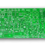
4-Layer EV Charger PCB: Design, Materials and Manufacturing Guide
A 4-layer EV charger PCB is increasingly common in AC charging stations, DC fast chargers, wall chargers, and commercial charging equipment because the control board must combine a microcontroller, communications, voltage and current sensing, relay and contactor drivers, temperature monitoring, protection, and human-machine interface functions in a compact space. Four copper layers provide more routing room, a continuous ground plane, cleaner power distribution, and a better foundation for EMC control than a conventional two-layer board.
This guide explains the stackup, materials, layout, thermal design, EMC, manufacturing, reliability, and cost factors involved in EV charger four-layer PCB production.
What Is a 4-Layer EV Charger PCB?
A four-layer PCB contains four copper circuit layers separated by core and prepreg dielectric materials and bonded through lamination. A common stackup places components and critical signals on the top layer, a continuous ground reference on layer two, power and auxiliary signals on layer three, and additional components and low-speed signals on the bottom.
This arrangement gives the control electronics a low-impedance return path for communication signals and a more direct power path for the various supply rails. It is especially useful when the charger includes CAN, RS-485, Ethernet, Wi-Fi, cellular, RFID, display interfaces, and isolated power circuits.
Why Four Layers Are Used in Charging Controllers
Adding layers increases available routing area, which reduces congestion when many functions are packed onto one control board. The continuous ground plane also lowers signal loop area and helps control electromagnetic radiation from relays, contactors, switching power circuits, and digital processors.
A dedicated power layer can distribute 3.3 V, 5 V, and other rails with lower impedance than long surface traces. This supports stable supply voltage for the MCU, communication chips, and analog sensors. Higher integration is another benefit because designers can place more components on a similar board footprint without forcing excessive routing through small channels.
Four layers do not solve EMC automatically. Good performance still depends on stackup, component placement, ground design, return current paths, isolation, filtering, and layout discipline.
Typical Stackup for EV Charger Control Boards
A practical four-layer stackup can start with L1 as the top signal and component layer, L2 as a complete ground plane, L3 as a power and auxiliary signal layer, and L4 as the bottom component and connector layer. The exact dielectric thickness and material must be defined with the board manufacturer so impedance targets can be calculated correctly.
For differential communication pairs such as Ethernet, CAN, or high-speed USB, the designer should confirm the target impedance with the selected prepreg thickness and dielectric constant. Copying a generic stackup can create impedance mismatch and signal integrity problems.
Copper weight should also be selected for the expected current. High-current paths may require heavier copper or wider traces, while control and communication circuits can use standard 1 oz copper.
Key Circuits on an EV Charger PCB
The MCU manages charging state, communication, fault detection, authentication, relay control, and monitoring. Communication interfaces include CAN, RS-485, Ethernet, Wi-Fi, Bluetooth, and cellular modules. Voltage and current sensing circuits measure the supply and charging parameters with appropriate scaling and isolation.
Protection circuits guard against overvoltage, overcurrent, overtemperature, short circuit, surge, ESD, and EFT events. Protection components should be placed close to the connectors and external interfaces where disturbances enter the board.
Relay and contactor drivers must be isolated from the low-voltage logic in a way that matches the product safety standard. Analog sensing, communication, and power-switching sections benefit from clear separation so switching noise does not corrupt sensitive measurements.
Material Selection for EV Charger PCBs
Standard FR-4 can satisfy many charger control boards when the operating temperature is moderate. High-Tg FR-4 is a common upgrade for EV charging equipment because it provides better thermal stability under heat cycling, lead-free soldering, dense component populations, and continuous operation.
Halogen-free laminate may be chosen for environmental compliance. If the control board carries high-speed Ethernet or wireless circuits, a laminate with stable dielectric properties can help maintain controlled impedance and signal quality.
The material choice should be confirmed early with the PCB manufacturing partner because dielectric thickness, copper roughness, and Tg affect both electrical performance and reliability.
Thermal Management and Power Integrity
Most charger control boards do not carry the full charging current, but DC/DC converters, MOSFETs, power-management ICs, relay drivers, and communication modules still generate heat. Copper area, thermal vias, component placement, and enclosure airflow should be considered together.
Power integrity depends on stable voltage for MCUs and communication devices. Decoupling capacitors should sit close to IC power pins, and high-frequency switching loops should be short. A dedicated ground plane and power plane make these loops smaller and reduce voltage ripple at sensitive devices.
EMC and Signal Integrity Considerations
Charging stations combine high power, high voltage, and digital control in one system, so EMC planning is essential. Noisy sections such as switching power supplies, relay drivers, and high-current switching paths should be separated from sensitive analog sampling, MCU, clock, and communication circuits.
High-frequency current loops should be small, and high-speed traces need a continuous reference plane. Avoid slots or splits under critical signals whenever possible. External interface protection should include TVS diodes and filtering close to connectors to reduce ESD, surge, and EFT damage.
A well-planned PCB design and layout review can catch return path, isolation, and filtering issues before fabrication.
Creepage, Clearance, and Isolation
Charging boards can work with mains voltage and high DC rails, so creepage and clearance requirements are important. The correct distances depend on operating voltage, overvoltage category, pollution degree, insulation type, and applicable standards.
High-voltage and low-voltage control regions must be separated according to safety requirements. Ground planes may need to be split or shaped around isolation boundaries, and the PCB supplier should understand where the isolation barrier must remain clean.
For sensitive power products, the complete system benefits from integrated energy electronics PCBA capability that covers board design, assembly, and test under one quality plan.
Manufacturing Process for Four-Layer Charger PCBs
Production begins with an engineering review of Gerber files, drill data, stackup, material, impedance requirements, and finish. Inner layers are imaged, etched, and inspected before lamination. Temperature, pressure, and time during lamination must be controlled to avoid delamination and dimensional shift.
Drilling creates through holes that will connect the layers. Electroless copper and electroplating build reliable copper in the hole walls. The outer layers are then imaged and etched, followed by solder mask, silkscreen, and surface finish.
Final inspection can include AOI, flying probe or electrical test, impedance test, dimensional check, microsection, and solderability testing. For charging equipment, the factory should also control processes that affect long-term thermal cycling and humidity resistance.
Reliability Requirements for Outdoor and Industrial Use
EV chargers may operate outdoors, in industrial locations, or in enclosures with wide temperature swings. Repeated thermal cycling can stress copper, vias, solder joints, and laminate material. PCB fabrication must therefore remain consistent from lot to lot.
Moisture and condensation are risks in outdoor equipment. The PCB should be compatible with the enclosure sealing level, and conformal coating or other protection may be used for sensitive control areas. For complete protection, conformal coating can be applied after assembly.
Cost of Four-Layer EV Charger PCBs
The cost of a four-layer charger PCB depends on size, layer count, material, copper weight, impedance requirements, finish, quantity, and test level. Standard FR-4 prototypes are relatively economical, while high-Tg material, controlled impedance, heavier copper, ENIG, and high-reliability testing increase the price.
Order quantity is also important. Prototype boards carry higher setup and engineering cost per unit, while volume production spreads those costs across more boards. A realistic production forecast lets the factory quote a more accurate price.
The stackup also affects production complexity. A four-layer board requires inner-layer imaging, lamination, and more registration work than a two-layer board, but these steps are well established and reliable when the supplier follows a controlled process. The final cost comparison should therefore include the expected yield and certification risk, not only the base PCB price.
Two-Layer or Four-Layer: Which Is Better?
A simple charging controller with a small number of functions and low communication speed may work on a two-layer board. When the design contains many interfaces, dense routing, high-speed signals, multiple power rails, or strict EMC requirements, four layers provide a better balance of performance and cost.
The decision should be based on component count, routing feasibility, signal integrity, EMI, thermal behavior, and the target product standard. Choosing four layers unnecessarily adds cost, while choosing too few layers can force poor layout compromises that appear only during certification or field use.
For reliable component sourcing during production, component procurement helps manage long-lead items such as connectors, relays, and isolated power modules.
When the board is qualified at prototype and then carried into higher volumes, the same stackup and design rules should remain under version control so manufacturing changes do not introduce unseen electrical or thermal differences.
Conclusion
A 4-layer EV charger PCB gives charging control electronics the routing density, ground integrity, power stability, and EMC control needed for modern communication and safety functions. Material, stackup, layout, manufacturing, and reliability must be evaluated together.
With an experienced design and manufacturing partner, EV charging OEMs can produce control boards that perform consistently in high-temperature, high-humidity, and high-power environments.