20-Layer ABF Substrate Guide: Structure, Materials, Process and Cost
What a 20-Layer ABF Substrate Is
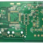
A 20-layer ABF substrate is a high density IC package substrate built with ABF build-up film as the dielectric, used to connect a semiconductor die to the PCB motherboard. AI processors, GPUs, CPUs, FPGAs, ASICs and high end network chips need enormous I/O counts and very clean high speed signaling, and the package substrate is where those connections are fanned out from the die to the ball grid. An ABF substrate carries ultra-fine traces, laser micro vias and sequential build-up layers that ordinary HDI boards cannot match, which makes it the interconnection platform under nearly every modern high performance chip. Understanding the structure, materials and process of this component helps engineers judge supplier capability, evaluate cost and avoid design decisions that wreck yield.
Why Advanced Chips Need 20 Layers
Compared with lower layer count substrates, a 20-layer design provides more routing area for the massive I/O of AI and HPC devices, better power integrity through dedicated plane pairs, cleaner signal integrity on controlled impedance layers, stronger EMI suppression and more uniform heat distribution. As chip integration rises and flip chip packages grow larger, the substrate must distribute power and ground across the whole die area while keeping thousands of high speed lanes short and consistent. Twenty copper layers arranged around a core give designers the routing channels, planes and via resources to satisfy that demand, which is why 20-layer and higher ABF substrates have become a requirement rather than a luxury for flagship computing products.
Typical Stack-Up Structure
A 20-layer ABF substrate normally uses a core plus build-up construction. A four to eight layer core is laminated first, then ABF build-up layers are added on both sides in a 6 plus 6 arrangement to reach about twenty total copper layers. The stack includes the core layers, ABF dielectric films, laser micro blind vias, copper filled via structures, power planes, ground planes, high speed signal layers and redistribution layers, with an ENIG or ENEPIG finish on the outer pads. Typical geometry is aggressive: line width and spacing around 8 to 12 micrometers, micro via diameters of 30 to 50 micrometers and stacked via chains two to four levels deep. That geometry is what fits thousands of connections into a package the size of a postage stamp while keeping impedance controlled.

Key Materials in ABF Substrates
Three material families define the ABF substrate. The first is the ABF build-up film itself, chosen for low dielectric constant, low loss factor, strong adhesion to copper foil, excellent laser drilling behavior, low moisture absorption, high dimensional stability and small high frequency signal loss. The second is ultra-thin high purity copper foil in weights around 9, 12 and 18 micrometers, which supports very fine lines, carries signals with low loss and keeps dimensions stable during processing. The third is the surface finish: ENIG, ENEPIG, immersion gold or selective gold plating. ENEPIG is especially valued for flip chip substrates because it provides both good solderability and reliable gold wire bonding on the same surface.
How a 20-Layer ABF Substrate Is Manufactured
Manufacturing follows a long sequence of precision steps. The multilayer core is laminated, drilled and imaged first. ABF film is applied under vacuum so the dielectric is void free, then CO2 or UV lasers form the micro blind vias. Electroplating fills those vias with copper to create reliable layer to layer connections, and the whole press, drill, plate, image cycle repeats in sequential build-up fashion until all twenty layers exist. Fine line formation relies on SAP or MSAP semi-additive processing to reach 10 micrometer scale traces, and every stage is guarded by AOI, X-ray registration checks and full electrical testing for continuity, isolation and impedance. Any drift in lamination pressure, laser energy or plating uniformity multiplies across twenty layers, which is why this product is manufactured only in tightly controlled facilities.
ABF Substrate vs HDI PCB
An ABF substrate is often compared with an HDI board, but they serve different jobs. An ABF substrate operates at finer line width and spacing, smaller micro vias, higher layer count in a thin package, and tighter dimensional control, and it uses build-up film dielectric tuned for high speed signals. An HDI PCB is a motherboard technology with more relaxed rules, larger features and lower cost per area. The substrate sits between the die and the HDI board, so a system can contain both: a demanding flip chip package on an ABF substrate mounted to an HDI motherboard. Choosing substrate grade processing for a motherboard, or ordinary PCB rules for a substrate, both end in failure.
Design Challenges in 20-Layer Substrates
Designing a twenty layer substrate demands control across many variables at once. Impedance must be held across tight geometry, differential pairs need matched lengths and spacing, the power delivery network needs low inductance planes, and crosstalk between dense lanes must stay within budget. Via stubs have to be minimized, thermal paths planned, the stack-up optimized, copper balance maintained to prevent warpage, and manufacturing tolerances respected. Warpage is a particular risk because a large thin substrate with mismatched copper can bow enough to break assembly yield. In practice the EDA team and the factory must work together on DFM from the first stack-up draft instead of discovering the problems on the first panel.
Where 20-Layer ABF Substrates Are Used
Twenty layer ABF substrates power the electronics at the center of the AI and communication boom. They carry AI accelerators, GPU graphics cards, server CPUs, FPGA platforms, custom ASICs, data center servers, high speed switches, cloud computing equipment and 5G infrastructure, and they are moving into automotive autonomous driving controllers as those systems demand more compute. The same technology is also the natural home for chiplet packaging, 2.5D integration and the early stages of 3D packaging, because those architectures multiply the number of die-to-die connections that only a high layer count, fine line substrate can route.
Manufacturing Standards
Because the end products run mission critical workloads, substrate fabrication follows the international standards used across the electronics industry. IPC-6012 covers rigid board performance, IPC-6018 addresses high frequency boards, IPC-4101 defines laminate and prepreg specifications, IPC-A-600 sets bare board acceptance criteria, IPC-2221 provides generic design rules and IPC-2226 applies specifically to build-up and high density interconnect designs. Specifying these documents and verifying the factory follows them keeps dimensional accuracy, electrical performance and long term reliability consistent between prototype and production.

ABF Substrate Price Considerations
ABF substrate price is high because the product combines expensive materials, exotic equipment and low yields relative to standard boards. Cost is driven by panel size, layer count, line and via precision, material grade and quantity. A prototype panel typically costs about $1,800 to $6,500, small volume production runs about $900 to $3,500 per panel, and volume pricing is quoted per project because annual quantity, process complexity and yield all move the number. The most effective way to reduce cost is DFM early: an optimized stack-up, balanced copper, realistic line rules and clean via planning raise yield and shorten development, which lowers the effective price of every good panel delivered.
DFM Advice for Substrate Projects
Teams developing a 20-layer ABF substrate should treat manufacturability as part of the electrical design. Optimize the stack-up before routing, plan micro via stacking and staggering deliberately, balance copper across the panel to fight warpage, control impedance targets with the chosen materials, route heat through planned thermal paths and keep line width and spacing inside the factory capability. Run signal integrity and power integrity simulation before release, verify material compatibility with the assembly profile, and perform a DFM review on the output files so that issues are fixed in the database rather than on the production floor. Sharing the design intent with the manufacturer during development instead of after quoting is the single biggest factor in a smooth ramp.
Working With Your Manufacturer
Substrate capability is not the same as ordinary PCB capability, so qualify the supplier carefully. Ask your PCB manufacturing partner whether it runs sequential build-up, laser micro via and SAP or MSAP processes, what minimum line width and via size it holds, and how many build-up layers it has produced in volume. Review warpage control, X-ray and AOI inspection and electrical test coverage, and confirm the quality system against the IPC documents listed above. Pair the substrate supplier with the SMT assembly and PCBA testing teams that will mount the final package, because a substrate that assembles poorly fails the whole module regardless of how well it was fabricated.
20-Layer ABF Substrate FAQ
Q1: What is an ABF substrate? An ABF substrate is a high density IC package substrate built with ABF build-up film that connects a chip to the PCB with fine lines and micro vias.
Q2: Why do AI chips need a 20-layer substrate? AI chips have very high I/O counts and extreme speed requirements, and twenty layers supply the routing space, power integrity and signal integrity those devices need.
Q3: How is an ABF substrate different from an HDI PCB? The substrate uses finer lines, smaller micro vias, tighter tolerances and build-up film dielectric, making it far more precise than an ordinary HDI motherboard.
Q4: What finish is used on ABF substrates? ENIG, ENEPIG, immersion gold and selective gold plating are common, with ENEPIG preferred for flip chip work that also needs wire bonding.
Q5: Why are 20-layer substrates expensive? The materials, precision equipment, long process flow and yield challenges make them costly, which is why DFM optimization early in the project is essential.
Conclusion
The 20-layer ABF substrate is the precision platform that lets modern CPUs, GPUs, AI accelerators and network ASICs deliver their performance. It combines ABF build-up film, ultra-thin copper and sequential build-up processing to create routing density and signal quality that standard HDI boards cannot reach. Teams that understand the stack-up, respect the design constraints and run DFM with the factory early will achieve better yield, lower cost and faster ramps. As chiplet and advanced packaging continue to grow, high layer count ABF substrates will only become more central to the electronics industry, and the PCB capabilities that support them will define what is possible in the next generation of computing hardware.