SMT Prototype Assembly Requirements: Proofing Guide
SMT prototype assembly requirements ensure that a proofing board is assembled correctly the first time. In the electronics industry, printed circuit boards are used as the mechanical and electrical base for almost every circuit. The prototype must verify both the design and the manufacturing process before the product is released for volume production.
PCB technology continues to improve. Trace widths are smaller, layer counts are higher, and design rules are updated so that smaller surface mount devices can be handled and soldered reliably. The prototype assembly process must follow these tighter requirements.
This guide explains the process requirements for SMT prototype proofing, component placement, and PCB material selection.
Purpose of SMT Proofing
Proofing is the process of building a small number of sample boards to validate the design before mass production. The sample boards are used for electrical test, mechanical fit, firmware development, and customer approval.
A prototype can reveal missing footprints, wrong pad sizes, signal integrity problems, and assembly issues. Correcting these problems at the prototype stage is much less expensive than correcting them after a large order.
The proofing process should represent the same production process as the final volume board. If the prototype uses different materials or process settings, the validation result may not be valid.
General Placement Requirements
Installed components must be placed accurately on the printed circuit board according to the assembly drawing and the board schedule. Each component should be placed at its designated pad location and orientation.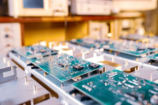
The type, model, and nominal value of every component must meet the requirements of the product assembly drawing and the component list. A wrong component in a prototype can hide a design problem or create a false failure.
All installed components must be intact. Damaged parts should not be used for prototype validation because they can create misleading test results.
Polarity markings should be checked before soldering. Reversed diodes, capacitors, and ICs may still be detected during test, but correcting them is slower than placing them correctly.
Solder End Immersion Requirement
The thickness of the solder end or solder leg of an SMT component that is immersed in the solder paste should not be less than half of the terminal height.
This requirement ensures that enough solderable surface contacts the paste to form a strong joint. If only a small part of the terminal enters the paste, the joint may have insufficient solder.
Component placement height should be controlled so that the terminal sits into the paste without squeezing all the paste from the pad.
For most components, the solder paste extrusion during placement should be less than about 0.2 millimeters. Fine-pitch parts should allow less than about 0.1 millimeters of paste extrusion.
Alignment and Centering
The soldering end or leg of the assembly should be aligned and centered with the pad pattern. Misalignment can reduce the wetting area and create weak or open joints.
Reflow soldering provides some self-alignment because the surface tension of molten solder pulls the component toward the correct pad position. A small placement deviation can therefore be corrected during reflow.
The allowable deviation depends on the component type and pitch. The relevant IPC standard should be used when the customer does not provide a specific limit.
If the initial deviation is too large, the self-alignment effect cannot correct it.
Inspect the Prototype Before Soldering
The prototype should be inspected immediately after component placement and before reflow. The operator should confirm that all parts are present, correctly oriented, and aligned with their pads.
A missing or misplaced component is easier to correct before soldering. Automated optical inspection or a simple visual check can be used depending on the component density.
The first prototype should be compared with the assembly drawing reference by reference. This check should be done by a second person to reduce the chance of missing an error.
After reflow, the board should be inspected again for soldering quality.
PCB Base Materials for Prototypes
Printed circuit boards can be made from several materials. The most widely used fiberglass substrate is FR-4. It provides a reasonable degree of stability under temperature changes at a moderate cost.
FR-4 is suitable for most digital and analog products. Lower-cost materials may be used for simple commercial boards where the performance requirement is not high.
For high-performance RF designs, the dielectric constant of the substrate is very important. Low-loss material is required, and PTFE-based printed circuit boards are often used even though they are more difficult to process.
The prototype material should match the final production material so the electrical results are valid.
Copper Clad Laminate
To form traces, the PCB factory starts with a copper-clad laminate. The laminate includes the substrate, usually FR-4, and copper foil on one or both sides.
Copper foil is bonded to the substrate and later etched to form the circuit pattern. The copper thickness and adhesion must support the trace width and current requirement.
FR-4 is normally easy to laminate and etch. PTFE is more difficult because its surface properties make copper adhesion harder, so PTFE processing needs special preparation.
Material selection affects impedance, thermal performance, and reliability of the assembled board.
SMT Proofing Documentation
The prototype order should include the PCB files, BOM, assembly drawing, and test instructions. Complete documentation prevents the factory from guessing component positions or polarity.
The engineer should also state the number of samples, the required surface finish, and the panelization preference.
A prototype may need extra boards for destructive testing or customer approval. The required quantity should be agreed before the order is placed.
All documentation should have the same revision number to avoid mixing old and new data.
Prototype Testing and Approval
After assembly, the prototype should be tested according to the product requirement. Functional testing verifies the complete circuit, while additional tests may be needed for signal quality or environmental performance.
The engineer should review the test results and compare them with the simulation or expected value. If a problem is found, the design should be corrected and a new prototype should be built.
The customer should approve the prototype before the design is released for volume production. Approval should include a written record of the tested samples and the decision.
Any change made after approval should create a new revision and require a new proofing cycle if the change affects the PCB layout.
A professional prototype PCB assembly service can build samples quickly while maintaining the process controls needed for accurate results.
Prototype assembly should be followed by PCBA testing so that the sample is verified before it is sent to the customer.
The proofing data should be stored with the quality management system and used as the baseline for the volume production process.
The board material and layout should be reviewed with PCB manufacturing and SMT PCB assembly engineers during the DFM check.
Assembly Schedule and First Article
The prototype assembly should follow the same process steps planned for volume production. The engineer should define the board loading direction, stencil design, placement sequence, and reflow profile before the first prototype is built. This makes the proofing result representative of the final production condition.
When the first prototype is completed, it should be treated as a first article. The board number should be recorded, and the operator should confirm that the assembly drawing, BOM, and process data were followed. The first article is then used as the reference for subsequent samples and repeat orders.
Quality Gates During Prototype Build
Prototype assembly should not skip quality gates simply because the quantity is small. Solder paste inspection, placement inspection, and post-reflow inspection are still important. A defect in a prototype can cause the engineer to make an unnecessary design change.
If the prototype has many hand-placed parts, the operator should mark each component on the assembly drawing as it is placed. This reduces the chance of a missing reference. The check should be reviewed by a quality inspector before the board is soldered.
After reflow, the board should be inspected under magnification. The inspector should look for bridges, opens, tombstoning, and misaligned parts. If a defect is caused by the placement process, the machine program should be corrected before the next prototype is made.
Repeat Prototype and Customer Approval
When the engineer makes a design revision, the prototype should be repeated with the new files. A small change in trace routing can create a new electrical problem, so the board cannot be approved based only on the previous revision.
The customer and factory should agree on the approval criteria before the proofing order starts. The criteria should include the number of tested samples, the acceptable test result, and the delivery condition. After approval, the same data should be used to build the pre-production and volume batches.
Every prototype revision should be stored with its photos, test data, and customer comments. This history helps the factory understand why a later production board behaves differently from the approved sample.
Conclusion
SMT prototype assembly requirements ensure that each component is placed correctly and that the board material matches the design. Placement, polarity, solder immersion, and alignment must be checked before reflow.
Proofing boards validate the circuit design, the PCB material, and the assembly process before volume production. Testing and customer approval complete the prototype cycle.
With careful proofing, the transition from sample to production is faster and more reliable.