




PCBA Component Damage Analysis: Crack and Stress Guide
PCBA component damage analysis helps engineers find out why a surface mount component cracked, lifted, or failed during assembly. As electronic products become more densely packed, the number of components on a single board increases and the risk of damage also increases. A damaged part can create an intermittent failure that is difficult to find in final test.
Component damage is usually caused by impact, bending stress, or thermal shock. The failure may occur during board handling, placement, reflow, testing, or assembly into the final product.
This guide explains common damage modes, how to read the crack shape, and how to protect PCB components during production.
Why Components Become Damaged
The main sources of component damage can be divided into operation issues and process damage. Operation issues include improper casing, poor board feeding, and manual bending of the clamped board.
Process damage includes impact fracture, stress damage, and delamination caused by thermal shock. Each failure mode creates a characteristic pattern on the component body and pad.
The assembly engineer should collect the failed part, the board position, and the process history before starting the analysis.
Damage Caused by Improper Support
When bending stress is applied to a component, adjacent supports can damage the part. The component may break or its electrode may peel from the body.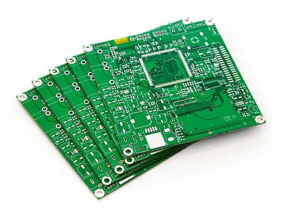
A damaged resistor often shows breakage or electrode peeling. A capacitor usually develops an inclined crack through its ceramic body.
If the damaged part is processed through reflow, the cracked component may separate or tombstone after the solder melts.
Support pins and board fixtures should be positioned so they do not press against components or create a bending fulcrum.
Stress Damage in Production
Poor board feeding can deform the PCB before it reaches the machine. Manual bending of the clamped board also applies stress to every component on the flexed area.
An improper suction nozzle or a placement height setting that is too low can press the component against the board and crack it.
Front-face cracking is a typical sign of this type of damage. The fracture often separates completely after the board passes through the reflow furnace.
If the side of the component is damaged, the impact point can often be identified by the cut or missing portion.
Impact Fracture
Lateral impact can damage a component without leaving an obvious impact point. The component may peel from the pad or its electrode may break.
Longitudinal impact is easier to identify. The impact point may show a missing corner on the part while the pad remains undamaged.
Impact can occur when boards are dropped, stacked, transported, or moved through a test fixture. Board separators and carriers should protect the components during every transfer.
Stress From Bending and Folding
Pressure and bending caused by folding the board edge, using a test fixture, or placing boards on a trolley can damage components. This type of damage usually appears as diagonal cracks.
Ceramic capacitors are particularly sensitive to board flex because their body is brittle. A small amount of board bend can create a crack that does not appear until thermal cycling.
The board should be supported and handled flat. Components should not be placed in high-flex areas such as near mounting holes and board edges.
Delamination From Thermal Shock
Improper soldering repair can cause layer stripping in a component. The typical feature is burnt black flux near the part, rough or discolored surface, and peeling of the capacitor layer.
Thermal shock can also occur when a board is heated too quickly or cooled too quickly during reflow.
Component manufacturing defects can also cause delamination. Poor interlayer bonding or an incorrect bake process may allow the internal layers to separate after reflow.
Rework should use controlled temperature and flux so that the component is not exposed to excessive heat.
Analyze the Impact Point
The presence of an impact point is not an absolute factor, but its location, direction, and damage level provide useful information.
A linear impact force usually damages the PCB first and creates visible defects on the components near the impact area.
A parallel impact force can crack or chip the component body directly. Because the torque direction is small, it may not damage the pad in most cases.
The engineer should examine the direction of the impact and compare it with the layout of surrounding components.
Analyze Crack Shape
Delamination cracks are usually caused by thermal shock. The internal layers separate and create a visible line inside the component body.
Inclined cracks are formed by bending stress. The lower part of the component becomes a fulcrum, and the fixed solder joint creates a crack at the electrode end. Large components perpendicular to the stress direction are most seriously affected.
Radial cracks usually come from point pressure. A casing, suction nozzle, or test fixture creates a small concentrated force on the component surface.
Complete fracture is the most serious mode. It is often accompanied by PCB damage and is usually caused by lateral impact or a severe capacitor crack.
Analyze Component Displacement
When a part has a longitudinal crack but has not separated, reflow heating can pull the crack open. The surface tension of the molten solder moves the damaged part and creates a tombstone.
Most of these failures are caused by component damage in the first process, bending stress, or improper ejector pin setting in the second process.
Cracks created by component cutting and packaging can also grow when the part is heated during reflow.
The analysis should therefore include the component supplier history as well as the assembly process.
Prevent Damage During Assembly
The PCB should be handled flat and supported during every process step. Board edges should not be folded or used as a handle.
Placement nozzles should be selected for the component size, and the placement height should be set so that the part is not pressed into the board.
Board support pins must avoid components and should be adjusted when the board is turned for second-side assembly.
Testing fixtures should use soft contacts and controlled force so that probes do not crack the component body.
The layout should keep brittle components away from board edges, mounting holes, and areas that flex during assembly. This rule should be included in the PCB design and layout guidelines.
During SMT PCB assembly, the placement machine and conveyor should be maintained so that boards are not bumped or bent.
After soldering, PCBA testing and inspection should find cracked parts before they are shipped. X-ray and AOI can support the optical inspection.
The assembly supplier should document every damaged component under quality management and use the analysis to improve the process.
Failure Analysis Workflow
The first step in analyzing a damaged component is to protect the evidence. The failed board should be handled gently and the damaged component should not be removed before photographs are taken. The photos should show the component, the pad, the crack direction, and the surrounding boards.
The engineer should then review the production route and process data. The board position number, the assembly date, and the machine settings can show whether the damage is random or repeated. A random failure may come from handling, while a repeated failure usually comes from a process condition.
Cross-section analysis can show whether the crack started inside the component or on the surface. The engineer may also use dye penetration testing to reveal a crack that is not visible from the outside.
The final report should identify the damage mode, the likely cause, and the corrective action. The report should be stored with the board history so that a later failure can be compared.
Component Design and Assembly Rules
Brittle components should be placed away from areas where the board is likely to flex. The designer should avoid placing a large ceramic capacitor directly across a board bend line. The pad geometry should support the component without creating unnecessary stress at the solder fillet.
Thermal relief should be used when a capacitor pad connects to a large ground plane. This reduces the temperature difference between the two terminations and lowers the risk of thermal cracking during reflow.
The assembly process should use a preheat stage that heats the board gradually. A rapid temperature change can crack a ceramic component even when no mechanical force is applied.
Rework stations should use hot air or hot tweezers with controlled temperature and should not drag a soldering iron across the component body.
Monitoring Damage Trends
The factory should track the number of cracked or missing components by board location. A control chart can show whether the damage rate is increasing after a machine adjustment or a change in the board support setup.
Incoming component inspection should also include a visual check for preexisting cracks. A component that arrives with a small internal defect may fail only after reflow, so the supplier history should be considered when the failure rate is high.
Damage data should be discussed in the quality review meeting. Corrective actions should be assigned to the process or design team and verified with a new production lot.
Continuous monitoring turns component damage from an unexpected field failure into a controlled manufacturing metric.
Conclusion
PCBA component damage analysis uses impact location, crack shape, and component displacement to identify the cause of the failure. Impact, bending stress, and thermal shock create different damage patterns.
Brittle components such as capacitors should be protected from board flex and point pressure. Board supports, nozzles, fixtures, and handling methods should be controlled.
With proper analysis and protection, the factory can reduce component damage and improve PCBA reliability.


