What Are BOM, DIP, SMT and SMD? PCB Assembly Terms Explained
Why PCB Assembly Terms Confuse New Buyers
Ordering a printed circuit board for the first time means meeting a collection of abbreviations: BOM, DIP, SMT, SMD, PCBA, DFM, and many more. Engineers use these PCB assembly terms every day, but buyers who come from a different background often find them difficult to separate. Understanding the basic vocabulary saves time during quotation and prevents expensive misunderstandings, because each term describes a real part of the design, the components, or the manufacturing process.
The four most frequent abbreviations are BOM, DIP, SMT, and SMD. Three of them describe physical things: a document, a package style, and a component type. The fourth, SMT, describes a method of assembly. Once these definitions are clear, technical conversations with a factory become much easier, and the buyer can follow discussions about placement, soldering, and inspection without guessing.
This guide explains each term in plain language, shows how the concepts connect in a real project, and highlights the questions buyers should ask when their product uses these technologies.
BOM: The Bill of Materials
The bill of materials, universally shortened to BOM, is a document that describes the structure of the product in a table format. For an assembled circuit board, the BOM lists every component with its reference designator, manufacturer part number, description, quantity, and sometimes the approved alternates. The BOM is the starting point for machine programming, component procurement, incoming inspection, and final quality validation, so an accurate BOM is the single most valuable file a customer can send to an assembly factory.
A poor BOM causes problems at every stage. If quantities are wrong, the line runs out of parts mid-batch. If part numbers are missing, procurement cannot order the correct components. If the reference designators do not match the layout file, the placement program places parts in the wrong positions. Professional assembly companies review the BOM against the Gerber files before production and confirm every discrepancy with the customer, which is one of the first quality checks in any serious project.
The BOM also drives cost. Component prices, lead times, and minimum order quantities all come from the BOM, and the buyer can reduce cost by allowing substitutes for commodity parts while restricting critical components to approved manufacturers.
DIP: Dual In-Line Package and Through-Hole Assembly
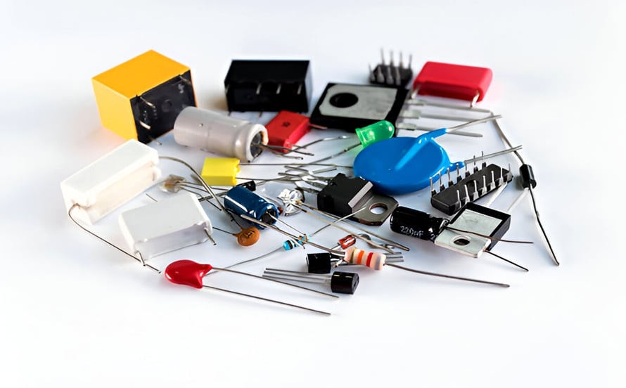
DIP stands for dual in-line package, a classic style of integrated circuit packaging. The chip is enclosed in a rectangular body with two parallel rows of pins, which are inserted into plated holes on the printed circuit board and soldered on the opposite side. Most small and medium integrated circuits can be produced in this package form, and the pin count is usually below one hundred. DIP components are robust and easy to handle, which made them the standard for decades of electronics manufacturing.
Assembling DIP parts belongs to through-hole technology. The pins are inserted into the holes, and the board is normally soldered with a wave soldering machine or selective soldering equipment. Through-hole joints are mechanically strong because the solder fills the barrel of the hole, which is why connectors, transformers, large capacitors, and parts exposed to vibration are still specified in DIP or other through-hole packages today.
The trade-off is density. Through-hole components occupy both sides of the board in a sense and require drilling, which makes the board larger and assembly slower than surface mount alternatives. Modern designs usually keep through-hole parts only where the mechanical or electrical benefit is real.
SMT: Surface Mount Technology
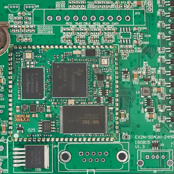
Surface mount technology, or SMT, is the method of assembling components onto the surface of the printed circuit board. The process starts with solder paste printed onto the pads through a stencil. A placement machine then positions the components on the pasted pads with high accuracy, and the board travels through a reflow oven where the paste melts, wets the pads, and solidifies into the solder joint. No holes and no pin insertion are required, which is the fundamental difference from through-hole assembly.
SMT production technology matured through the 1980s. Mass production of surface mount components drove prices down sharply, and capable machines became affordable, so the method spread across the entire electronics industry. Because surface mount parts are small and can be placed on both sides of the board, SMT increases assembly density, reduces product size and weight, and supports fully automated production. A surface mount assembly is typically far lighter and smaller than its through-hole equivalent, while delivering the same function.
The applications are everywhere. Aviation electronics, communication equipment, computers, medical electronics, automotive electronics, office automation, and household appliances all rely on SMT. The technology also enables the high pin counts and fine pitch of modern integrated circuits, which simply cannot be achieved with packages designed for manual insertion.
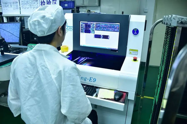
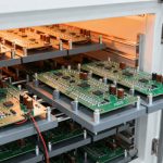
A complete SMT line is a chain of machines rather than a single oven. Solder paste is printed and its volume checked by a solder paste inspector, components are placed by high-speed and high-accuracy mounters, the board passes through reflow, and automated optical inspection verifies the result. Each station reports data that process engineers use to keep the line stable, and the same line can switch between different products in minutes by loading a new program and a new stencil.
SMD: Surface Mount Device
A surface mount device, or SMD, is any component designed to be assembled with surface mount technology. Early electronic boards were assembled with through-hole parts, first completely by hand and later with machines that placed simple leaded components while complex parts still needed wave soldering and manual work. The introduction of surface mount components changed the industry: passive components, active devices, and integrated circuits were redesigned with small terminals or solder balls on their bodies, allowing automatic pick-and-place machines to assemble them all.
Today the range of SMDs is enormous. Resistors, capacitors, inductors, diodes, transistors, LEDs, connectors, and complex integrated circuits are all available in surface mount form. The abbreviation appears in package names such as SMD resistor or SMD capacitor, and it also appears when engineers contrast the older leaded parts with the newer chip-style parts.
The distinction between SMT and SMD is simple once separated: SMT is the assembly technology, SMD is the component type. A factory performs SMT assembly using SMD components, and the machines that place them are part of the SMT line.
SMD packages range from tiny chip resistors and capacitors measured in hundredths of an inch to large ball grid array integrated circuits with hundreds of solder balls under the body. Between those extremes sit QFP packages with leads on four sides, small outline transistors, LED packages, and connector families built for surface mounting. The variety is the reason placement machines need multiple nozzle types and vision systems to recognize every part before placement.
How These PCB Assembly Terms Work Together
A real product usually combines all four concepts. The customer provides the design files and the BOM, which lists SMD components for the surface mount portion of the board and perhaps a few DIP connectors or through-hole parts for mechanical strength. The factory programs its placement machines from the BOM and the layout, assembles the SMD components with SMT processing, then adds the through-hole parts and finishes them with selective or wave soldering.
Inspection follows the same logic. The SMT portion is checked with automated optical inspection after reflow, while through-hole joints are verified visually or with X-ray when hidden under components. The testing stage then proves that the assembled board works as designed. Understanding these terms lets a buyer follow this chain and ask meaningful questions at every handoff point.
Terminology also affects cost. A board described as all-SMT is usually cheaper to assemble in volume than a board with many through-hole parts, because the SMT process runs automatically while through-hole work adds machine time or manual labor. Designers who understand the trade-offs can often reduce cost simply by choosing the right package style for each function.
The same vocabulary applies whether the project is a prototype of ten boards or a production run of one hundred thousand. In a prototype, the buyer may ask the factory to hand-place a few DIP parts while the SMD portion runs through the SMT line. In volume production, the same mixed assembly is automated with selective soldering for the through-hole joints, and the BOM controls the component stock from the first article to the last batch.
How gopcb Applies These Technologies
gopcb supports every combination of these PCB assembly terms in one place. The company manufactures the bare board, checks the BOM with its procurement team, runs SMD components through its SMT lines, and handles DIP and through-hole work with wave and selective soldering when the design requires it. Because the whole flow is managed internally, mixed-technology boards do not suffer from handoffs between separate vendors.
The same team provides PCB manufacturing, SMT PCB assembly, and through-hole PCB assembly, with components procurement managed against the approved BOM. Every board is inspected and tested before shipment under the turnkey PCB assembly service model, and the customer receives the files, records, and reports needed for a smooth product launch.