SMD Chip Thrust Test: Standards and Methods for PCB Assembly
Why the Chip Thrust Test Matters in PCB Assembly
Soldered components look the same from the outside whether the joint is strong or weak, which is why PCB assembly factories cannot rely on visual checks alone. The SMD chip thrust test measures the actual adhesion strength of a soldered component by pushing it sideways until the joint fails. The measured force tells the quality engineer whether the solder paste, the reflow profile, the pad finish, and the placement process together produced a mechanically sound connection. A reliable factory treats the test as a production gate, not as a formality, and keeps the results available whenever a question about board quality arises.
The test is also known as a shear or push test, and it belongs to the family of solder joint reliability checks used in incoming inspection, process qualification, and routine production monitoring. Weak joints that escape this kind of test can break later during handling, vibration, or thermal cycling, causing intermittent failures in the field that are expensive to trace. Testing early is far cheaper than discovering the problem after the product reaches the customer.
This article explains when to run the chip thrust test, how to perform it correctly, the typical force standards for common SMD components, and the precautions that keep the results meaningful.
When the Adhesion Test Should Be Performed
Routine testing starts when a production line is transferred or set up for a new order. The in-process quality control team performs the adhesion thrust test on SMD components of different specifications from the first boards produced, so that a weak process is detected before a large batch is soldered. The same test is repeated at defined intervals during long production runs, because solder paste age, stencil wear, and reflow drift can degrade joint strength gradually without producing visible defects.
Testing is also triggered by change. A new solder paste batch, a different stencil, a revised reflow profile, a new board surface finish, or a substituted component all justify additional chip thrust tests. Some customers define the test frequency and the acceptance forces in their own quality agreements; when no customer specification exists, the factory follows relevant quality standards or the IPC general inspection criteria.
Sampling should cover the component types that are most critical for the product: large packages that carry mechanical loads, components near board edges, and parts whose failure would disable the whole circuit. Testing a representative mix of small passives and larger packages gives a realistic picture of overall soldering quality.
Standard Procedure for the Chip Thrust Test
The procedure starts with preparation. The thrust gauge must be reset to zero before the measurement so that the pointer or digital display reads zero on the scale. The test is performed on a supported board so that the PCB does not flex under the applied force, because board bending would absorb part of the load and falsify the result. The operator selects the appropriate tool or probe for the component size and positions the assembly under the gauge.
Force is applied at an angle of thirty to forty-five degrees to the board surface. The operator pushes the component at a uniform speed so that the reading reflects steady adhesion strength rather than the shock of a sudden impact. Fast application is explicitly avoided, because a quick strike can damage the component or produce a reading that does not represent normal solder joint quality. The maximum force reached before the joint fails is the recorded value.
Every result is written on the inspection record sheet, and the operator notes the component type, the machine and shift that produced the board, and the measured force. Boards with failed components are marked, separated from the good material, and sent for repair; after rework the components are re-tested before the board returns to the production flow.
Typical Force Requirements by Component
Acceptance forces follow the size and mass of the component, because a large part naturally requires more force to shear than a tiny chip. Common reference values used in production lines are 0.8 kilograms for 0603 chip components, 1.0 kilogram for 0805 components, and 1.5 kilograms for 1206 components. Diodes in chip packages are typically required to withstand more than 1.5 kilograms, transistors more than 2.0 kilograms, and integrated circuit packages more than 3.0 kilograms.
These numbers are practical starting points rather than universal limits. The correct acceptance value for a specific product should be agreed between the customer and the factory, because the required strength depends on the board material, the pad design, the solder alloy, and the mechanical environment of the final product. When in doubt, the IPC general inspection standards provide a consistent reference that both sides can accept.
It is equally important to define what a test failure means. A single weak component may indicate a local problem such as a contaminated pad, while several failures across the board point to a process issue such as insufficient paste, an incorrect profile, or poor solderability of the parts. The factory should investigate the cause before rework, otherwise the same defect will reappear in the next batch.
SMT vs Through-Hole: The Context of Bond Strength
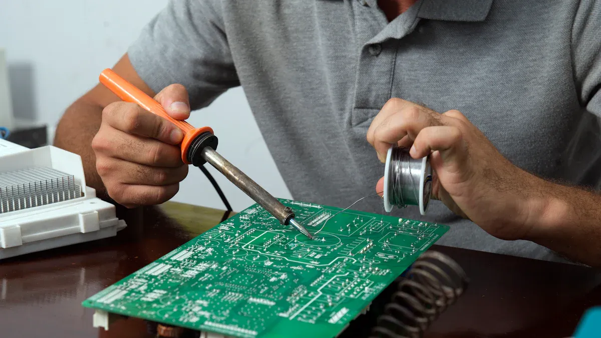
Surface mount components rely entirely on the solder joint for mechanical support, which is why adhesion testing is so important. Through-hole components are different: their leads are inserted into plated holes and soldered on the opposite side, so the solder fills the barrel of the hole and creates a strong mechanical lock. Through-hole assembly has been used since the earliest circuit boards and is extremely reliable under mechanical stress, but it requires drilling, uses both sides of the board for the joint, and limits the routing space below the top layer.
SMT was developed to use board area efficiently and reduce manufacturing cost. Components with metal terminations or end caps are soldered directly to pads on the surface, without drilling and without leads passing through the board. Parts can be smaller and placed on both sides, automation is easier, and highly complex circuits fit into compact products. The trade-off is that the solder joint alone carries the mechanical load, which makes joint quality and its verification central to surface mount reliability.
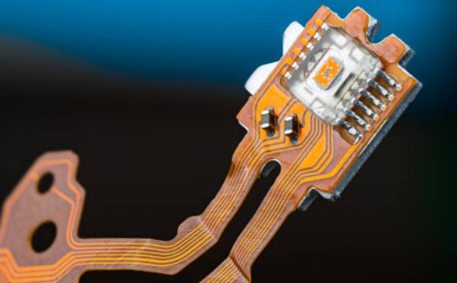
Board technology changes the test requirements as well. Flexible and rigid-flex circuits, for example, place the solder joints close to bend zones where mechanical stress concentrates, so adhesion strength is even more critical and the test method may need to be adapted to avoid damaging the flex substrate. Assemblies that combine SMD components with through-hole parts also need a test plan that covers both technologies, because the failure modes are different even when the product works correctly at first.
Modern boards usually combine the two technologies. Small components and integrated circuits are placed with SMT for density and speed, while connectors, large capacitors, and parts exposed to vibration or heavy use remain in through-hole packages for mechanical strength. The chip thrust test verifies the SMT portion, and the through-hole joints are controlled through solder quality checks of their own.
Precautions That Keep Results Meaningful
The most common error in chip thrust testing is applying force too quickly. A sudden impact loads the component like a hammer blow and can crack the part or the board rather than testing the solder joint, so the operator must push at a controlled, uniform speed. The gauge must be reset before every measurement, and the board must be supported underneath the test point so that flexing does not share the load.
The angle of the applied force also needs discipline. Pushing at the specified thirty to forty-five degrees reproduces the direction of real mechanical loads, while an angle that is too flat or too steep produces numbers that cannot be compared with the standard. Operators should be trained and the test station should be checked regularly, because the value of the test depends entirely on consistent execution.
Records complete the loop. Without written results the test gives no protection, because nobody can prove that a batch was verified or trace a failure back to the shift that produced it. Inspection sheets should identify the board, the components, and the line conditions, and the records should be kept with the batch documentation that is delivered to the customer.
How gopcb Verifies Solder Joint Reliability
gopcb includes adhesion testing in its routine quality checks for SMT production. After line setup and at planned intervals during production, the quality team performs chip thrust tests on the agreed component types, compares the results with the applicable standards, and keeps the inspection records with the batch files. Any weakness found is traced back to the process through the production data before rework begins.
The same discipline covers the whole chain: PCB manufacturing, SMT PCB assembly, PCBA testing, and PCB assembly for mixed technology boards, all documented under the quality management system. Send gopcb your design files and quality requirements to discuss the inspection plan, including turnkey PCB assembly services that cover the complete production flow.