The rapid development of modern electronics has driven continuous miniaturization of electronic components and the widespread adoption of SMT Assembly technology. Modern SMT Manufacturing lines are highly automated and require high positioning accuracy, fast production speeds, and consistent process control.
As automation continues to increase, PCB Design must be developed with the requirements of automated assembly equipment in mind. A PCB that does not meet the mechanical and process requirements of an SMT production line may reduce production efficiency, increase defects, or even prevent automatic assembly from being completed.
For this reason, successful PCB Design is not limited to electrical performance. Board dimensions, component placement, fiducial marks, clamping areas, panelization, and manufacturing tolerances must also be considered during the design stage.
What Is SMT Assembly?
SMT Assembly, or Surface Mount Technology Assembly, is an advanced electronic manufacturing process in which surface-mount components are placed directly onto designated PCB pads and soldered to the board.
Compared with traditional Through-Hole Technology (THT), SMT provides a higher level of automation and is particularly suitable for high-volume electronic production. SMT also supports smaller components, higher component density, shorter electrical connections, and more compact product designs.
A typical automated SMT Manufacturing line may include:
- PCB loader
- Solder paste printer
- Solder paste inspection (SPI) system
- Pick-and-place machine
- Reflow soldering oven
- Automated optical inspection (AOI) equipment
- PCB unloader
The PCB is transported through the production line by conveyors or rails. Solder paste is first printed onto the pads, components are then accurately placed, and the assembled PCB passes through the reflow oven to form reliable solder joints.
The effectiveness of this automated process depends heavily on whether the PCB has been designed to work correctly with the production equipment.
How PCB Design Affects SMT Manufacturing
PCB Design is an important link between the electronic design and the physical SMT Manufacturing process. A circuit may be electrically correct, but the PCB can still create production problems if its mechanical dimensions, component placement, or manufacturing features are unsuitable for automated assembly.
The main PCB design factors that should be considered for SMT production include:
- PCB outline and shape
- PCB size and thickness
- Conveyor and clamping requirements
- Fiducial marks
- Component keep-out areas
- Board-edge clearance
- Panelization
- V-Cut or tab-routing connections
- Component orientation
- Solder pad design
- Assembly-side identification
- Manufacturing tolerances
These requirements should be considered before PCB fabrication rather than being corrected after production begins.
PCB Pattern and Board Outline
In an automated SMT Assembly line, the PCB moves through multiple machines on a conveyor system. Therefore, the board outline must be compatible with the equipment’s transportation and clamping mechanism.
A standard rectangular PCB is generally easy to transport because its straight edges provide stable contact with conveyor rails and clamping mechanisms.
However, irregular PCB outlines can create mechanical interference. For example, recessed sections, large cutouts, unusual corners, or non-linear board edges may prevent the conveyor system from gripping the PCB correctly.
If an irregular outline is necessary because of the product’s mechanical requirements, designers can consider adding temporary rails or extending the board outline in the production panel. These areas can later be removed through depanelization.
Rounded corners or chamfered corners may also be used when required by mechanical design, but the final outline should always be checked against the actual SMT equipment and PCB handling method.
PCB Size and Thickness
PCB Size must fall within the working range of the SMT equipment used for production. The exact minimum and maximum dimensions vary according to the specific printer, pick-and-place machine, conveyor, reflow oven, and handling system.
Therefore, there is no single universal PCB size requirement for every SMT production line.
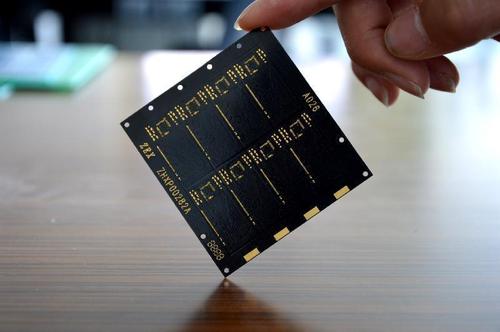
Very small PCBs may require panelization or the use of manufacturing rails so that the board can be transported reliably through the equipment.
Large and thin PCBs require additional attention because they may be more susceptible to warpage during reflow soldering. Excessive board deformation can affect component placement accuracy, solder paste printing, and conveyor transport.
For this reason, the relationship between board length, width, thickness, material construction, copper distribution, and reflow conditions should be evaluated during PCB Design.
For small boards, multiple individual PCBs can be combined into one production panel. The appropriate panel configuration depends on board dimensions, thickness, component placement, depanelization method, and the capabilities of the SMT line.
PCB Positioning and Fiducial Marks
Accurate positioning is essential for automated SMT Assembly.
SMT machines use mechanical references and optical recognition systems to determine the position and orientation of the PCB. Among these features, Fiducial Marks are especially important for high-precision component placement.
A fiducial mark is a clearly defined optical reference feature that allows SMT equipment to identify the actual position of the PCB and compensate for manufacturing tolerances or small positional deviations.
Common design considerations include:
- Shape: A solid circular mark is commonly preferred because it provides a clear and easily recognizable optical reference.
- Size: The exact fiducial size should follow the requirements of the assembly equipment and PCB manufacturer. A commonly used design is approximately 1 mm in diameter, but this should not be treated as a universal requirement.
- Surface: The fiducial should provide a stable and consistent optical contrast. It should not be covered by solder mask or contaminated by surrounding markings.
- Clearance: A clear keep-out area should be provided around the fiducial to prevent interference from copper, silkscreen, solder mask openings, pads, or other visual features.
For high-density and fine-pitch boards, global and local fiducials may both be required. Local fiducials can provide additional positional references for fine-pitch components such as BGAs, QFNs, and other high-density packages.
Component Clearance Along the PCB Edge
Component placement near the PCB edge is another important factor in PCB Design for automated assembly.
During SMT production, the board is normally held and transported by conveyor rails or clamps. Components located too close to the clamping edge may interfere with the equipment or become damaged during transportation.
Therefore, designers should establish a component keep-out zone along the edges used for conveyor support.
The required clearance depends on:
- SMT equipment configuration
- Conveyor rail width
- Clamping mechanism
- Component package size
- Component height
- PCB thickness
- Panelization method
- Assembly sequence
Components should not be placed blindly according to a generic edge-clearance number. The actual requirements should be confirmed with the PCB assembly manufacturer.
If components must be located close to the board edge, production rails or temporary extension areas can be added to provide sufficient mechanical clearance.
PCB Panelization
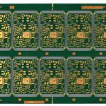
PCB Panelization combines multiple individual PCBs into a larger manufacturing panel. This is particularly useful for small boards because it improves handling efficiency and allows multiple boards to pass through the SMT line as one production unit.
Panelization can provide several benefits:
- Better automated handling
- Higher production efficiency
- Reduced loading and unloading operations
- Improved utilization of PCB materials
- More consistent assembly processing
- Lower manufacturing cost in suitable production volumes
The panel arrangement should be designed according to the PCB shape, component distribution, assembly direction, and depanelization process.
Common PCB panelization methods include:
- V-Cut
- Tab routing
- Perforated or routed tabs
- Hybrid routing structures
V-Cut and Tab Routing
V-Cut is commonly used when individual boards have relatively straight edges. A controlled groove is formed on both sides of the PCB, allowing the boards to be separated after SMT assembly.
However, the remaining PCB material must be sufficient to maintain panel strength during transportation and reflow.
If the V-Cut depth is excessive, the panel may become mechanically weak and could crack or separate prematurely during handling. If the remaining material is too thick, depanelization may require excessive force and can stress the PCB or components.
Tab routing is another common panelization method. Small tabs keep individual boards connected within the panel and are cut or routed away after assembly.
The appropriate method depends on the PCB material, thickness, board geometry, component placement, and depanelization equipment.
Marking and Silkscreen Design
In addition to Fiducial Marks, the PCB may contain reference designators, polarity indicators, logos, barcodes, and other markings.
These markings should not interfere with optical inspection or component placement.
In particular, silkscreen text or lines should not overlap fiducial marks. Excessive copper, solder mask openings, or other visual features around the fiducial can also reduce recognition reliability.
Poor marking design may result in repeated machine recognition errors, unnecessary production stoppages, and reduced SMT Manufacturing efficiency.
A clean and consistent PCB marking strategy therefore contributes to both automated assembly and inspection.
Component Placement for Automated SMT
Component placement should be considered from both electrical and manufacturing perspectives.
Components should be positioned so that:
- Pick-and-place nozzles can access them reliably.
- There is sufficient spacing between adjacent components.
- Polarity and orientation are clear.
- Tall components do not interfere with nearby components.
- Components do not interfere with board-edge clamps.
- Fine-pitch components have sufficient assembly clearance.
- Rework and inspection remain practical.
Component orientation should also be considered when the PCB passes through the SMT line. Consistent orientation can simplify machine programming and improve production efficiency.
For high-density assemblies, the designer should also consider component height, shadowing effects, thermal distribution, soldering accessibility, and the inspection requirements of AOI or X-ray systems.
Pad Design and Soldering Considerations
Although the SMT machine controls component placement, reliable solder joints depend heavily on PCB pad design.
The pad geometry should correspond to the component manufacturer’s recommended land pattern whenever possible. Incorrect pad dimensions can lead to solder bridging, insufficient solder, component displacement, tombstoning, or poor solder-joint reliability.
For fine-pitch packages, designers should pay particular attention to:
- Pad dimensions
- Pad-to-pad spacing
- Solder mask clearance
- Solder paste aperture design
- Thermal pad configuration
- Via placement
- Component courtyard
- Reflow behavior
PCB pad design should therefore be coordinated with stencil design and the solder paste printing process.
PCB Design and SMT Equipment Compatibility
Modern SMT Equipment provides high-speed and high-precision automated manufacturing, but equipment performance depends on the quality and consistency of the PCB being processed.
Before releasing a PCB for production, designers should verify:
- PCB dimensions are compatible with the SMT line.
- Board thickness is suitable for transportation and reflow.
- The board outline provides adequate clamping surfaces.
- Fiducial marks are correctly designed and positioned.
- Components maintain sufficient clearance from board edges.
- Panelization is compatible with the selected depanelization process.
- V-Cut or routing structures provide adequate panel strength.
- Component placement supports automated pick-and-place.
- PCB pads are compatible with stencil printing and soldering.
- Silkscreen and other markings do not interfere with optical recognition.
Early verification can prevent costly production modifications.
The Role of DFM in PCB Design
Design for Manufacturing (DFM) is especially important when developing PCBs for automated SMT Assembly.
A PCB should not only function electrically; it should also be manufacturable, inspectable, and suitable for automated production.
A practical DFM review should evaluate:
- PCB dimensions
- Board thickness
- Material selection
- Layer stackup
- Copper distribution
- Component spacing
- Board-edge clearance
- Fiducial marks
- Pad geometry
- Solder mask
- Silkscreen
- Panelization
- Assembly access
- Testing requirements
Working with the PCB manufacturer and assembly provider at an early stage allows potential manufacturing problems to be identified before the PCB enters mass production.
How Kingda Supports SMT-Oriented PCB Manufacturing
At Kingda, PCB development can be evaluated from both electrical design and manufacturing perspectives. By considering PCB fabrication, assembly requirements, panelization, component placement, and production constraints together, designers can reduce avoidable manufacturing issues and improve production consistency.
For complex or high-density boards, early communication between the designer and manufacturer is particularly valuable. This allows key parameters such as board dimensions, stackup, tolerances, surface finish, fiducial requirements, panel structure, and assembly constraints to be reviewed before production.
Conclusion
The development of automated electronics manufacturing has made SMT Assembly a fundamental production technology for modern electronic products. At the same time, increasingly automated SMT Manufacturing places higher demands on PCB Design.
A successful PCB design must consider more than circuit functionality. PCB Size, board outline, component clearance, Fiducial Marks, panelization, clamping areas, pad geometry, and compatibility with SMT Equipment all influence manufacturing efficiency and assembly quality.
By incorporating DFM principles into the design process and communicating with the PCB manufacturer at an early stage, companies can reduce production risks, improve assembly efficiency, and achieve more consistent product quality.
For reliable high-volume production, PCB Design, PCB Manufacturing, and SMT Assembly should be treated as interconnected stages of the same manufacturing process rather than isolated activities.