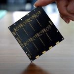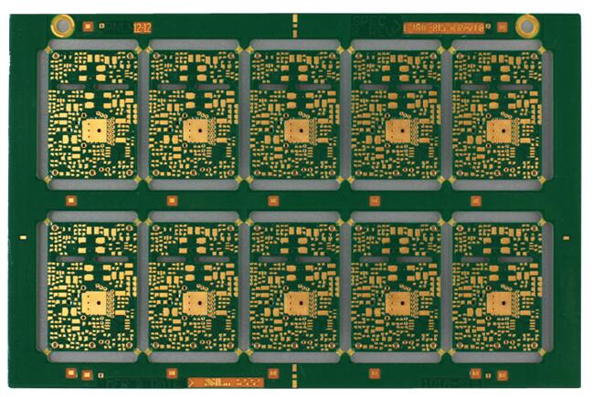
A PCB Circuit Board provides the physical foundation for electronic components and electrical interconnections in an electronic product. Even when the schematic is electrically correct, an improperly designed PCB can negatively affect signal quality, thermal performance, manufacturability, and overall product reliability.
For this reason, PCB Design should not focus only on whether the circuit connections are correct. Designers must also consider component placement, routing, power distribution, grounding, thermal management, electromagnetic compatibility, mechanical constraints, and manufacturing requirements.
A well-planned PCB Layout helps shorten critical signal paths, control unwanted coupling, improve heat dissipation, simplify assembly, and reduce potential sources of electrical and mechanical failure.
1. Basic Principles of PCB Design
Before beginning a PCB Layout, designers should establish the board dimensions, mechanical constraints, major functional areas, and locations of critical components.
The following principles should be considered during PCB Design.
1.1 Consider PCB Size and Mechanical Constraints
PCB dimensions should be determined according to the enclosure, component requirements, electrical performance, manufacturing process, and thermal conditions.
An unnecessarily large board may increase routing length, material consumption, and manufacturing cost. Longer traces can also increase parasitic resistance, inductance, and susceptibility to coupling in high-speed or sensitive circuits.
On the other hand, making a PCB unnecessarily small can create problems such as:
- Limited component placement space
- Insufficient trace spacing
- Poor thermal spreading
- Difficult routing
- Increased electromagnetic coupling
- Reduced assembly and inspection accessibility
Therefore, PCB size should be optimized rather than simply minimized.
Before starting detailed PCB Layout, designers should first identify the mechanical envelope and the locations of connectors, mounting holes, heat-generating components, switches, displays, and other mechanically constrained parts.
1.2 Place High-Frequency Components Carefully
High-frequency circuits require particularly careful component placement.
The connections between critical high-frequency components should generally be kept short and direct. Shorter interconnects can reduce parasitic inductance and capacitance and help control signal integrity.
Components that are particularly sensitive to interference should be separated from major noise sources such as:
- High-speed clocks
- Switching regulators
- Power converters
- High-current switching nodes
- RF transmitters
- Fast digital interfaces
Input and output paths should also be arranged carefully to reduce unwanted coupling and feedback.
For high-speed interfaces, the complete signal path—including the source, transmission line, vias, connector, load, and return-current path—should be considered rather than evaluating the trace in isolation.
1.3 Maintain Appropriate Electrical Clearance
When two conductors or components operate at significantly different voltages, adequate electrical clearance must be provided to reduce the risk of arcing or unintended short circuits.
The required spacing depends on factors such as:
- Working voltage
- Transient or peak voltage
- Pollution degree
- Insulation material
- Altitude
- Applicable safety standard
- Manufacturing capability
High-voltage components should also be positioned where accidental contact is minimized during testing, debugging, assembly, and servicing.
For safety-critical products, PCB Design should distinguish between clearance—the shortest distance through air—and creepage—the shortest distance along an insulating surface.
1.4 Consider Mechanical Support for Heavy Components
Large or heavy components should not rely solely on solder joints for mechanical support when their weight or mechanical loading could exceed the capability of the soldered connections.
Components such as large transformers, power inductors, heat sinks, relays, connectors, and other mechanically stressed parts may require additional mechanical support.
The appropriate solution can include:
- Mechanical brackets
- Screws or fasteners
- Chassis support
- Adhesive reinforcement
- Board-mounted supports
The actual requirement depends on component mass, vibration, shock, mounting orientation, and product environment rather than a universal component-weight threshold.
1.5 Separate Heat-Generating Components
Components that generate substantial heat should be positioned according to the thermal design of the entire product.
Power semiconductors, voltage regulators, high-current resistors, transformers, inductors, and other heat-generating components should not unnecessarily heat temperature-sensitive devices.
During PCB Design, designers should consider:
- Copper area
- Thermal vias
- Heat sinks
- Airflow
- Component spacing
- Thermal interface materials
- Chassis conduction
- Ambient temperature
Thermal design should be evaluated together with electrical and mechanical requirements rather than treated as a separate process.
1.6 Consider Adjustable Components and User Access
For adjustable components such as potentiometers, variable inductors, variable capacitors, switches, and calibration devices, their accessibility should be determined by the final product structure.
If an adjustment must be performed directly on the PCB during production or service, the component should be placed where it can be accessed safely and conveniently.
If the adjustment is intended to be performed from the product exterior, its PCB location should correspond to the position of the external control or adjustment mechanism.
This approach helps avoid unnecessary mechanical modifications after PCB fabrication.
1.7 Reserve Mounting Holes and Mechanical Keep-Out Areas
Mounting holes occupy physical space and can affect surrounding copper, traces, components, and ground structures.
During PCB Layout, designers should reserve sufficient keep-out areas around mounting holes and mechanical supports.
Depending on the product, designers may also need to consider:
- Screw heads
- Spacers
- Washers
- Standoffs
- Chassis walls
- Connector clearance
- Heat sinks
- Cable routing
Mechanical constraints should therefore be incorporated before detailed routing begins.
2. PCB Layout Requirements for EMI and Noise Control
In addition to mechanical considerations, PCB Design must address electromagnetic interference and unwanted electrical coupling.
A good PCB Layout can significantly reduce noise by controlling current paths, minimizing unnecessary loop areas, separating incompatible circuit functions, and maintaining appropriate reference planes.
2.1 Arrange Functional Blocks According to Signal Flow
A practical layout usually begins by dividing the circuit into functional blocks, such as:
- Power input and power conversion
- Analog circuitry
- Digital processing
- High-speed interfaces
- RF circuitry
- Clock generation
- Power amplification
- Sensor interfaces
Each functional block should be positioned according to the actual signal and power flow.
Critical signal paths should generally be kept short and direct. At the same time, the designer should avoid creating routing arrangements that force return currents to take unnecessarily long paths.
For high-speed circuits, signal routing and return-current paths should always be considered together.
2.2 Place Components Around Functional Centers
Within each functional block, major components should be placed according to their electrical relationships.
For example, a switching regulator should keep its input capacitor, switching components, inductor, and output capacitor appropriately positioned to minimize high di/dt loop area.
Similarly, high-speed interface components should be placed so that the signal path from the transceiver to the connector or receiver is as direct as practical.
This component-level planning can reduce unnecessary routing and simplify subsequent PCB Routing.
2.3 Keep High-Speed and Sensitive Circuits Properly Separated
High-speed signals can generate electromagnetic coupling through electric fields, magnetic fields, common impedance, and shared return paths.
Sensitive analog or low-level circuits should therefore be positioned away from strong switching-noise sources whenever practical.
Particular attention should be given to:
- Clock signals
- DDR and other high-speed memory interfaces
- USB and PCIe-class high-speed interfaces
- Switching power supplies
- RF circuits
- ADC/DAC interfaces
- Low-level sensor signals
However, separation alone is not sufficient. Effective EMI Control also requires appropriate grounding, reference planes, stackup design, trace geometry, filtering, and return-path management.
2.4 Minimize Unnecessary Parallel Routing
Long parallel traces can increase crosstalk through capacitive and inductive coupling.
Therefore, designers should avoid unnecessarily routing sensitive traces in parallel with:
- High-speed clocks
- High-current switching nodes
- Fast digital signals
- RF transmission lines
- Noisy power traces
Where parallel routing cannot be avoided, designers can use appropriate spacing, reference planes, ground shielding structures, differential routing, or layer changes according to the signal type and stackup.
The correct solution depends on the frequency, trace geometry, dielectric structure, routing length, and impedance requirements.
2.5 Use Reference Planes and Controlled Return Paths
For high-speed signals, the return current tends to follow a path associated with the signal’s electromagnetic field and reference structure.
An uninterrupted reference plane can therefore be extremely valuable for maintaining a predictable return path and controlling electromagnetic coupling.
During High-Speed PCB Design, designers should avoid unnecessarily routing high-speed traces across:
- Plane splits
- Large voids
- Reference-plane discontinuities
- Poorly connected copper regions
If a signal changes reference layers, an appropriate return-current transition should also be considered.
This is particularly important for high-speed differential and single-ended interfaces.
2.6 Consider PCB Shape and Aspect Ratio
A rectangular PCB is often convenient for manufacturing, assembly, enclosure integration, and automated handling. However, there is no universal requirement that every PCB must follow a specific length-to-width ratio.
The appropriate board shape depends on:
- Product enclosure
- Component placement
- Connector locations
- Mounting requirements
- Manufacturing panelization
- Thermal management
- Signal routing
- Mechanical strength
For larger PCBs, especially those with relatively low thickness, mechanical rigidity should be evaluated carefully. Board thickness, material selection, copper distribution, mounting locations, and support points can all influence warpage and mechanical stability.
2.7 Maintain Adequate Spacing Between Functional Areas
The physical arrangement of different circuit blocks should reflect their electrical compatibility.
For example, a power conversion section may be positioned away from low-level analog circuitry, while an RF section may require controlled routing and shielding from digital switching noise.
However, functional separation should not result in unnecessarily long signal or return paths.
The objective is to achieve an appropriate balance between:
- Electrical isolation
- Short signal paths
- Controlled return currents
- Thermal performance
- Mechanical integration
- Manufacturing efficiency
3. PCB Routing Considerations
After component placement is established, PCB Routing should be performed according to electrical priorities rather than simply filling available space.
Important routing considerations include:
Signal Integrity
High-speed traces should be designed with appropriate impedance, reference-plane continuity, length control, and via structures.
Power Integrity
Power distribution networks should provide low and controlled impedance over the relevant frequency range. Decoupling capacitors should be placed according to the current path and the power-delivery requirements of the device.
Crosstalk Control
Trace spacing and routing direction should be selected to limit unwanted coupling between neighboring signals.
Grounding
Ground connections should provide appropriate return paths and minimize unnecessary loop areas. A ground strategy should be based on circuit behavior rather than simply dividing analog and digital grounds without considering return-current paths.
Thermal Management
High-current traces, power planes, thermal vias, and copper areas should be coordinated with the thermal design of the PCB.
Manufacturability
Trace width, spacing, via dimensions, copper thickness, solder mask clearance, and other features must remain within the actual capabilities of the selected PCB manufacturer.
4. PCB Reliability and Manufacturing Considerations
A reliable PCB Circuit Board must satisfy electrical, mechanical, thermal, and manufacturing requirements simultaneously.
Before releasing a design for production, designers should perform a comprehensive review covering:
- Schematic-to-layout connectivity
- Component footprints
- Component orientation
- Trace width and spacing
- Electrical clearance and creepage
- Via structures
- Power and ground routing
- Thermal paths
- Board-edge clearance
- Mounting holes
- Connector positions
- Manufacturing tolerances
- Assembly accessibility
- Inspection requirements
Design Rule Check (DRC) should be performed before manufacturing, but automated DRC should not replace engineering review.
For high-speed designs, signal integrity and power integrity analysis may also be required. For products with strict electromagnetic compatibility requirements, EMI Control should be considered from the earliest design stage.
5. Best Practices for a Reliable PCB Layout
The following checklist provides a practical starting point for PCB Design:
- Define mechanical dimensions and mounting requirements first.
- Divide the circuit into clear functional blocks.
- Place critical and high-frequency components before general-purpose components.
- Keep high-speed signal paths short and continuous.
- Provide appropriate return-current paths.
- Separate sensitive circuits from major noise sources.
- Minimize unnecessary parallel routing.
- Keep high di/dt power loops compact.
- Provide adequate thermal paths for power components.
- Maintain appropriate clearance around mounting holes and PCB edges.
- Verify footprints against component manufacturer documentation.
- Check component accessibility for assembly and rework.
- Review the design against actual PCB manufacturing capabilities.
- Perform DRC and, where necessary, SI, PI, thermal, and EMC analysis.
Kingda’s Approach to PCB Design and Manufacturing
At Kingda, a manufacturable PCB starts with a well-planned design. PCB layout decisions can affect fabrication, assembly, inspection, reliability, and overall production efficiency.
For complex boards, early communication between the designer and manufacturer can help identify potential issues related to board construction, stackup, trace geometry, via structures, component clearance, thermal requirements, and manufacturing tolerances.
By integrating PCB Design, PCB Layout, PCB Routing, manufacturing requirements, and reliability considerations into one workflow, designers can reduce avoidable production problems and improve the consistency of the final electronic product.
Conclusion
The quality of a PCB Circuit Board depends not only on whether the schematic is electrically correct but also on how effectively the circuit is translated into a physical layout.
A professional PCB Layout should balance electrical performance, signal integrity, power integrity, thermal management, mechanical requirements, EMI Control, and manufacturing capability.
By applying sound PCB Design principles, carefully planning component placement, controlling routing and return-current paths, and reviewing manufacturability before production, designers can build PCBs that are easier to manufacture, assemble, test, and maintain while achieving better overall reliability.