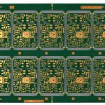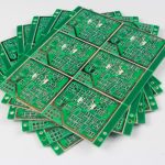
As electronic products continue to operate at higher data rates and frequencies, High-Speed PCB Design has become increasingly important. At high frequencies, a PCB trace can no longer be treated simply as an ideal wire. Its physical geometry, dielectric environment, reference plane, length, vias, and surrounding conductors can all affect signal behavior.
One of the most important considerations in high-speed circuit design is Controlled Impedance. Maintaining a predictable impedance along a signal path helps reduce reflections, signal distortion, timing uncertainty, and other signal-integrity problems.
A successful PCB Design therefore requires more than correct schematic connections. Designers must coordinate the PCB stackup, trace geometry, reference planes, component placement, routing, vias, grounding, and manufacturing tolerances.
1. Understanding Transmission Lines on a PCB
A transmission line can be understood as a signal conductor together with its associated return-current path.
The return path is not necessarily a conventional ground wire. In a multilayer PCB, for example, a signal trace routed on one layer may use an adjacent power or ground reference plane as part of its electromagnetic return path.
Therefore, a PCB transmission line generally consists of:
- Signal conductor
- Dielectric material
- Reference conductor or plane
- Distributed capacitance
- Distributed inductance
This structure determines the Characteristic Impedance of the transmission line.
For a uniform transmission line, the goal is to maintain a consistent electrical environment along the critical signal path. Changes in trace width, dielectric thickness, copper thickness, reference-plane spacing, vias, connectors, or layer transitions can cause impedance discontinuities.
These discontinuities may produce reflections and degrade Signal Integrity.
2. What Is Characteristic Impedance?
Characteristic Impedance is an inherent electrical property of a transmission line. It describes the voltage-to-current relationship of a traveling wave on a uniform transmission line.
A simplified relationship is:
[
Z_0 \approx \sqrt{\frac{L’}{C’}}
]
where:
- (Z_0) is characteristic impedance
- (L’) is inductance per unit length
- (C’) is capacitance per unit length
This simplified relationship helps explain why the physical construction of a PCB affects impedance.
For example, increasing trace width generally increases capacitance and changes inductance. Increasing the distance between a signal trace and its reference plane also changes the electromagnetic field distribution and therefore changes the effective impedance.
Consequently, Controlled Impedance is fundamentally a combination of electrical design and physical construction.

3. How a Signal Travels Along a Transmission Line
Consider a voltage step applied to one end of a transmission line.
The voltage does not instantly appear at the other end. Instead, an electromagnetic wave propagates along the transmission line at a velocity determined primarily by the dielectric environment and field distribution.
In a typical PCB structure, propagation velocity is slower than the speed of light in vacuum because the electromagnetic field interacts with the dielectric material.
As the signal propagates, electric and magnetic fields are established around the signal and its return path. The transmission line behaves as a distributed network of inductance and capacitance rather than as a single lumped component.
This is why a long PCB trace can exhibit transmission-line behavior even though it looks like a simple copper conductor.
The exact propagation velocity depends on the effective dielectric constant of the structure and the transmission-line geometry.
4. Why Controlled Impedance Matters in High-Speed PCB Design
At relatively low frequencies and short interconnect lengths, a PCB trace can often be approximated as a lumped electrical connection.
As signal rise time becomes faster, however, even signals with relatively modest clock frequencies can contain significant high-frequency spectral components.
When the electrical length of an interconnect becomes significant compared with the signal rise/fall time, transmission-line effects become increasingly important.
Poor impedance control can result in:
- Signal reflections
- Ringing
- Overshoot and undershoot
- Increased jitter
- Reduced eye opening
- Timing errors
- Increased electromagnetic emissions
- Receiver detection problems
Therefore, High-Speed PCB Design should evaluate signal rise time, interconnect length, topology, package effects, connectors, vias, and the complete channel rather than relying only on nominal clock frequency.
5. Controlled Impedance PCB Structures
Common PCB transmission-line structures include microstrip and stripline.
Microstrip
A microstrip consists of a signal trace on an outer PCB layer with a reference plane below it.
Its impedance is influenced by:
- Trace width
- Copper thickness
- Dielectric thickness
- Dielectric constant
- Solder mask
- Reference-plane geometry
Because part of the electromagnetic field is exposed to air, the effective dielectric environment differs from a stripline.
Stripline
A stripline is generally routed between reference planes within the PCB stackup.
The surrounding dielectric and reference planes provide a more controlled electromagnetic environment. Stripline structures can therefore be useful for high-speed and sensitive signals where consistent impedance and electromagnetic containment are important.
The exact stackup should be designed according to the target impedance, material properties, fabrication capability, and routing requirements.
6. PCB Stackup and Impedance Control
A properly designed PCB Stackup is one of the foundations of Controlled Impedance.
Important parameters include:
- Layer count
- Copper thickness
- Dielectric thickness
- Dielectric constant
- Prepreg construction
- Core thickness
- Trace width
- Trace spacing
- Reference-plane position
For example, if the distance between a signal layer and its reference plane changes significantly, the trace impedance may also change.
Therefore, designers should not define impedance only by trace width. Trace width must be evaluated together with the complete PCB stackup.
The final impedance should also account for manufacturing tolerances. A nominal design value is not sufficient if the production process cannot consistently reproduce the required geometry.
7. PCB Routing for High-Speed Signals
PCB Routing is one of the most important parts of High-Speed PCB Design.
High-speed traces should be routed with attention to the complete electromagnetic path.
Key considerations include:
- Maintain a continuous reference plane.
- Minimize unnecessary routing length.
- Avoid unnecessary layer transitions.
- Control trace spacing.
- Minimize discontinuities.
- Avoid unnecessary stubs.
- Keep high-speed differential pairs appropriately coupled.
- Maintain consistent impedance.
- Provide a suitable return-current path.
The shortest route is not always the best route. A slightly longer route with a continuous reference plane and fewer discontinuities can perform better than a shorter route with poor return-current continuity.
8. Return-Current Path
One of the most commonly overlooked aspects of PCB Routing is the return-current path.
A signal and its return current form a complete electromagnetic circuit. At high frequencies, the return current tends to concentrate in the region associated with the signal’s electromagnetic field and reference structure.
If a high-speed trace crosses a large split or void in its reference plane, the return path may be disrupted.
This can increase loop area, electromagnetic coupling, and signal distortion.
Therefore, during PCB Design, designers should ensure that high-speed signals have an appropriate and continuous reference structure whenever practical.
If a signal must change reference layers, an appropriate return-current transition should be considered.
9. Vias and Impedance Discontinuities
Vias are essential for connecting different PCB layers, but they can introduce parasitic capacitance and inductance.
A via structure may also create a discontinuity because the signal transitions through:
- Different copper geometries
- Different dielectric environments
- Via barrels
- Anti-pads
- Nearby reference structures
For very high-speed signals, via stubs can also become significant.
Designers can reduce via-related discontinuities through techniques such as:
- Minimizing unnecessary vias
- Optimizing via diameter
- Controlling anti-pad dimensions
- Using back-drilling where appropriate
- Using blind or buried vias when justified
- Optimizing layer transitions
The appropriate approach depends on signal speed, rise time, stackup, board thickness, manufacturing capability, and cost.
10. Differential Pair Routing
Differential signaling is widely used in high-speed interfaces because it can provide good common-mode noise rejection and controlled signal transmission when properly implemented.
During PCB Routing, designers should maintain:
- Appropriate differential-pair spacing
- Consistent geometry
- Similar routing environments
- Continuous reference structures
- Controlled impedance
- Reasonable intra-pair skew
Abrupt changes in spacing or routing geometry can create impedance discontinuities.
Differential pairs should also avoid unnecessary separation between the positive and negative conductors because the coupling between them is part of the intended transmission-line structure.
11. Trace Width and Spacing
Trace width is an important parameter in Controlled Impedance design, but there is no universal trace width that applies to every PCB.
The required width depends on:
- Target impedance
- Dielectric thickness
- Dielectric constant
- Copper thickness
- Signal-layer structure
- Reference-plane position
- Manufacturing tolerance
- Frequency and rise time
Trace spacing also affects crosstalk.
Long parallel routing between aggressive signals and sensitive signals should be minimized where possible. If parallel routing is necessary, designers should evaluate spacing, reference planes, routing length, and the expected coupling.
12. General PCB Design Rules
In addition to high-speed requirements, general PCB design rules should be established to support reliable fabrication and assembly.
Typical considerations include:
Trace Width
Minimum trace width should be determined according to the PCB manufacturer’s process capability and the electrical requirements of the circuit.
For high-current applications, trace width should also be evaluated together with copper thickness, allowable temperature rise, current duration, and thermal environment.
Trace-to-Trace Spacing
Clearance should be selected according to signal voltage, safety requirements, manufacturing capability, and the applicable product standard.
A single fixed spacing value should not be treated as suitable for every PCB.
Copper-to-Board-Edge Clearance
Copper should normally maintain an appropriate distance from the board edge to prevent exposed copper and manufacturing damage.
The required clearance depends on PCB fabrication capability and the mechanical construction of the product.
Component-to-Board-Edge Clearance
Components should be positioned with sufficient clearance from the board edge to avoid interference with:
- PCB clamps
- Conveyor rails
- Depanelization
- Enclosures
- Fasteners
- Assembly equipment
13. Pad Design and Teardrops
Pads are critical connection points between PCB traces and component terminals.
Pad geometry should be based on the component package, manufacturer-recommended land pattern, soldering process, and electrical requirements.
Teardrop structures may be used at certain trace-to-pad or trace-to-via transitions.
A teardrop gradually widens the connection between the trace and pad or via, which can improve manufacturing robustness in some designs and reduce sensitivity to registration variation.
However, teardrops should be applied according to actual design and manufacturing requirements rather than automatically to every pad.
For through-hole components, finished hole diameter should provide sufficient clearance for the component lead and manufacturing process.
The appropriate annular ring and pad dimensions depend on the component lead, plating process, drill tolerance, and PCB fabrication capability.
14. Via Design
Vias should be used efficiently in a professional PCB Design.
Unnecessary vias increase routing complexity and may introduce additional electrical discontinuities.
When a via is required, designers should consider:
- Finished hole size
- Pad diameter
- Annular ring
- Aspect ratio
- Current-carrying requirement
- Layer transition
- Anti-pad geometry
- Clearance from surrounding features
Power and ground vias may need larger or multiple structures when carrying significant current.
For high-current paths, the number and arrangement of vias should be evaluated according to current distribution and thermal requirements rather than relying on a single fixed via size.
15. Silkscreen and Overlay Design
The silkscreen, or overlay layer, provides information that helps with assembly, inspection, troubleshooting, and maintenance.
Typical information includes:
- Component reference designators
- Polarity indicators
- Pin-1 indicators
- Connector labels
- Test-point identifiers
- Product markings
- Manufacturing information
Silkscreen should not overlap solder pads or obscure important component identification.
Text should also be positioned so that it remains visible after components are assembled.
A visually attractive silkscreen is useful, but readability and manufacturing practicality are more important than simply achieving uniform text placement.
16. SMD Component Considerations
Surface-mount devices have specific layout requirements because their terminals are typically distributed around the component body or underneath the package.
For SMD components, designers should verify:
- Correct footprint
- Pin-1 orientation
- Package dimensions
- Land pattern
- Courtyard
- Component height
- Assembly clearance
- Rework accessibility
For packages such as QFN and BGA, some solder joints may not be directly visible after assembly. Therefore, the footprint, stencil aperture, thermal pad design, and inspection method should be coordinated carefully.
17. Solder Mask and Paste Mask
Solder mask and paste mask serve different functions in PCB manufacturing.
Solder Mask
The solder mask protects copper from environmental exposure and helps prevent unintended solder bridging during assembly.
Solder-mask openings around pads should be designed according to the pad geometry and PCB fabrication capability.
Paste Mask
The paste mask defines the solder-paste stencil openings used during SMT assembly.
Paste-mask apertures may need to be modified for:
- Fine-pitch components
- QFN thermal pads
- Large pads
- Uneven component geometry
- Special soldering requirements
The paste aperture should therefore be considered together with stencil thickness, solder paste properties, component package, and reflow conditions.
18. Copper Pour and Plane Areas
Large copper areas can be used for:
- Ground distribution
- Power distribution
- Thermal spreading
- EMI control
- Current carrying
- Reference-plane construction
Designers should distinguish between solid copper planes and hatched copper areas because they may have different electrical, thermal, mechanical, and manufacturing effects.
For high-speed designs, continuous reference planes are generally preferred where they are required to maintain predictable return-current paths.
For high-current circuits, copper area and copper thickness should be selected based on current, temperature rise, thermal path, and manufacturing capability.
19. Analog and Digital Grounding
A common design mistake is to assume that analog and digital grounds must always be physically separated.
In reality, the appropriate grounding strategy depends on the system architecture.
The primary objective is to control return-current paths and prevent noisy currents from flowing through sensitive circuit regions.
Depending on the application, designers may use:
- A continuous ground plane
- Functional grounding regions
- Carefully controlled return paths
- Local filtering
- Ground stitching
- Galvanic isolation
- Separate power domains
The grounding strategy should therefore be determined from actual current flow and system requirements rather than applying a universal “split ground” rule.
20. Flying Wires and Unrouted Nets
During PCB development, “flying lines” can refer to temporary graphical connections representing unrouted nets.
These connections are useful during component placement because they show the electrical relationships between components before routing is completed.
Designers can use them to:
- Optimize component placement
- Reduce unnecessary trace crossings
- Improve routing efficiency
- Identify unconnected nets
After routing, remaining flying lines can indicate nets that have not yet been properly connected.
In professional PCB Design, unrouted connections should normally be resolved in the PCB layout itself rather than relying on physical jumper wires.
Jumper wires may be acceptable in certain prototypes or special applications, but they are generally undesirable for high-volume automated manufacturing because they add assembly complexity and reduce production consistency.
21. PCB Layout for Manufacturing
Good PCB Manufacturing begins with a manufacturable design.
Before releasing the PCB for fabrication, designers should review:
- Minimum trace width
- Minimum spacing
- Hole sizes
- Annular rings
- Board thickness
- Copper thickness
- Solder mask clearance
- Silkscreen placement
- Board-edge clearance
- Component clearance
- Panelization
- Surface finish
- Controlled-impedance requirements
Manufacturing limits should be agreed with the selected PCB manufacturer before finalizing the design.
A design that is technically possible but difficult to manufacture may result in lower yield, longer production cycles, or higher cost.
22. Controlled Impedance and PCB Manufacturing
Controlled impedance is not purely a PCB layout issue. It is a manufacturing requirement as well.
The final impedance depends on actual production characteristics, including:
- Copper thickness
- Trace width
- Dielectric thickness
- Material dielectric properties
- Etching variation
- Lamination thickness
- Registration accuracy
Therefore, the designer and PCB manufacturer should establish the impedance target and construction together.
For impedance-critical boards, impedance coupons or other verification methods may be used to confirm that the manufactured PCB meets the required electrical characteristics.
23. High-Speed PCB Design Checklist
Before releasing a high-speed PCB for manufacturing, designers should verify the following:
- Define the target impedance for critical interfaces.
- Establish the PCB Stackup before detailed routing.
- Select appropriate PCB materials.
- Calculate or simulate transmission-line geometry.
- Maintain consistent reference planes.
- Control trace width and spacing.
- Minimize unnecessary vias and stubs.
- Review differential-pair routing.
- Check return-current continuity.
- Minimize discontinuities at connectors and layer transitions.
- Evaluate crosstalk between critical signals.
- Review power distribution and decoupling.
- Perform DRC before fabrication.
- Use SI simulation when required.
- Confirm impedance requirements with the PCB manufacturer.
24. Kingda’s Approach to High-Speed PCB Manufacturing
At Kingda, high-speed PCB production should be considered as an integrated process from material selection and stackup planning to fabrication and electrical verification.
For impedance-sensitive boards, manufacturing capability is particularly important because small variations in trace geometry, dielectric thickness, copper thickness, or registration can influence the final electrical performance.
Early communication between the PCB designer and manufacturer can help establish:
- Target impedance
- Layer stackup
- Material construction
- Copper thickness
- Trace geometry
- Via structures
- Manufacturing tolerances
- Impedance verification requirements
This design-for-manufacturing approach helps reduce unnecessary iterations and supports more consistent high-speed PCB production.
Conclusion
High-Speed PCB Design requires designers to consider the PCB as an electromagnetic structure rather than simply a collection of copper wires.
Characteristic Impedance is determined by the relationship between trace geometry, dielectric materials, reference planes, and manufacturing construction. Maintaining Controlled Impedance therefore requires coordination between circuit design, PCB Stackup, PCB Routing, signal integrity analysis, and PCB Manufacturing.
A reliable high-speed PCB should provide controlled transmission-line structures, continuous return-current paths, appropriate via transitions, suitable grounding, and manufacturable geometries.
By integrating signal-integrity requirements with practical manufacturing constraints from the beginning, designers can reduce reflections, crosstalk, EMI problems, and production risks while achieving more stable high-speed electronic performance.