Designing a mixed-signal PCB requires a clear understanding of how analog and digital circuits interact. Unlike a purely digital or purely analog board, a mixed-signal PCB contains circuits with very different noise tolerances, signal characteristics, return-current behavior, and electromagnetic coupling mechanisms.
A successful Mixed-Signal PCB Design therefore cannot rely on a single layout rule. Designers need to consider the complete signal path, including the source, transmission path, return path, power distribution network, sensitive circuits, and potential coupling mechanisms.
Understanding these fundamentals makes it easier to establish appropriate PCB Layout, routing, grounding, filtering, shielding, and power-distribution strategies. It also helps designers identify and control Crosstalk before it becomes a system-level performance problem.
1. Analog and Digital Signals Have Different Noise Tolerances
One of the most important concepts in Mixed-Signal PCB Design is that analog and digital circuits generally respond differently to interference.
Digital Signal Immunity
A digital receiver normally interprets a signal according to defined logic thresholds. As long as the received voltage remains within the required logic-high or logic-low region, a certain amount of noise may not change the logical state.
For example, a digital signal with a nominal voltage of 3.3 V may tolerate a certain amount of noise without causing a logic error, depending on the receiver’s input thresholds, noise margins, timing requirements, and operating conditions.
This does not mean that digital circuits are immune to noise. Excessive noise can still cause:
- False switching
- Timing errors
- Jitter
- Data corruption
- Electromagnetic interference
- Power integrity problems
However, digital systems often have a relatively well-defined noise margin.
Analog Signal Sensitivity
Analog circuits are different because interference can directly degrade the information contained in the signal.
An analog receiver may not simply determine whether a signal is above or below a logic threshold. Instead, the amplitude, phase, frequency, linearity, noise floor, and distortion of the signal may all affect system performance.
Low-level analog signals can therefore be extremely sensitive to interference generated by nearby digital circuits.
For example, high-gain amplifier inputs, sensor interfaces, ADC inputs, DAC outputs, RF front ends, and precision reference circuits may be affected by very small coupled noise voltages.
As a result, Analog Signal paths generally require much more careful noise control than ordinary digital interconnects.
2. Why Analog Circuits Can Be Extremely Sensitive
The sensitivity of an analog circuit is often determined by its required signal-to-noise ratio (SNR), dynamic range, resolution, gain, bandwidth, and application environment.
A small amount of interference may become significant after amplification or signal processing.
This is particularly important in high-resolution ADC and DAC applications.
For an ideal N-bit converter, the theoretical quantization-limited SNR is approximately:
SNR ≈ 6.02N + 1.76 dB
For an ideal 14-bit converter, this gives approximately 86 dB of theoretical SNR.
In a real system, however, the effective number of bits (ENOB), reference noise, clock jitter, power-supply noise, thermal noise, layout, grounding, and other non-ideal effects reduce actual performance.
Therefore, it is not appropriate to assume that every 14-bit ADC or DAC automatically requires the same PCB noise specification. The actual requirement depends on the complete system architecture.
The important design principle is that Analog Signal integrity can be much more sensitive to interference than digital logic-state detection.
3. Digital Signals Can Be Strong Noise Sources
Digital circuits are not necessarily the victims of interference. They can also be major noise sources in a mixed-signal system.
Fast digital transitions contain significant high-frequency spectral content. Even when the fundamental clock frequency is relatively low, a fast rise or fall time can generate substantial high-frequency components.
Common noise sources include:
- High-speed clocks
- DDR interfaces
- High-speed serial links
- Switching regulators
- DC/DC converters
- Digital processor interfaces
- High-current transient loads
- Fast GPIO signals
The problem becomes more serious when large transient currents flow through shared power or ground structures.
For example, a switching current can generate voltage noise according to the relationship:
V = L × di/dt
where:
- V is the transient voltage,
- L is the effective inductance of the current path,
- di/dt is the rate of current change.
This is why minimizing high-frequency current-loop inductance is an important part of PCB Grounding and power integrity.
4. The Fundamental Objective of Mixed-Signal PCB Design
The goal of Mixed-Signal PCB Design is not to completely eliminate every interaction between analog and digital circuits.
That is usually neither practical nor necessary.
Instead, the objective is to control the noise source, coupling path, and victim circuit so that interference remains below the system’s allowable limit.
A useful framework is the classic:
Source → Coupling Path → Victim
Noise Source
Potential sources include:
- Switching power supplies
- Digital clocks
- High-speed data buses
- Processor interfaces
- Oscillators
- Power converters
- Large transient currents
Coupling Path
Noise can reach a sensitive circuit through:
- PCB traces
- Power planes
- Ground structures
- Shared return paths
- Parasitic capacitance
- Mutual inductance
- Electromagnetic radiation
- Connectors and cables
Victim Circuit
Sensitive circuits may include:
- ADC inputs
- DAC outputs
- Operational amplifier inputs
- Voltage references
- Sensor interfaces
- RF receivers
- Low-noise amplifiers
- Audio circuits
- Precision measurement circuits
Effective EMI Control requires identifying all three elements rather than focusing only on the victim circuit.
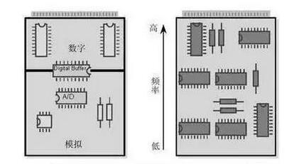
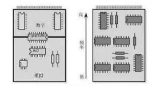
5. PCB Partitioning for Analog and Digital Circuits
Functional partitioning is one of the first steps in a reliable PCB Layout.
Analog and digital circuits should be arranged according to their functional relationships and noise sensitivity.
A typical mixed-signal board may contain:
- Digital processing section
- High-speed interface section
- Analog signal-conditioning section
- ADC/DAC section
- Power conversion section
- RF section
- Clock generation section
High-noise circuits should be physically separated from sensitive analog circuits whenever practical.
For example, a switching regulator should generally not be placed immediately next to a precision voltage reference or a low-level amplifier input.
However, partitioning does not mean that the PCB should always be divided into completely isolated analog and digital ground planes.
The correct strategy depends on the signal-return paths and system architecture.
6. Control Return Current Paths
Return-current management is one of the most important aspects of PCB Grounding.
At high frequencies, current tends to follow paths determined by the electromagnetic field and the impedance of the available return network. A signal trace therefore cannot be considered independently from its return path.
If a high-speed digital trace crosses an inappropriate plane boundary or is forced to take a long return path, the resulting loop area and discontinuity can increase electromagnetic coupling.
For this reason:
- Keep high-speed signal paths over an appropriate reference plane.
- Minimize unnecessary return-path discontinuities.
- Avoid routing sensitive analog traces through noisy digital regions.
- Provide low-impedance return paths for high-frequency currents.
- Carefully evaluate layer transitions and reference-plane changes.
Good return-path design can significantly reduce unwanted coupling without relying solely on physical separation.
7. Avoid Unnecessary Parallel Routing
One of the most common sources of Crosstalk is long parallel routing between aggressor and victim traces.
When two traces run close together, electromagnetic coupling can occur through both electric and magnetic fields.
Crosstalk generally increases with:
- Greater parallel-routing length
- Smaller spacing
- Faster signal edges
- Stronger driver output
- Higher mutual capacitance
- Higher mutual inductance
Therefore, sensitive analog traces should not run parallel for long distances with high-speed digital clocks or switching-node traces.
If routing proximity cannot be avoided, designers can consider:
- Increasing trace spacing
- Reducing parallel length
- Adding an appropriate ground reference
- Changing routing layers
- Improving return-current continuity
- Using shielding structures where appropriate
The actual spacing should be determined by stackup, trace geometry, signal rise time, impedance requirements, and acceptable coupling level rather than relying on one universal spacing ratio.
8. Keep High-Noise Power Circuits Away From Sensitive Analog Circuits
Switching power supplies can generate significant high-frequency noise.
The most sensitive areas include:
- Switching nodes
- Inductor current loops
- Diode or synchronous-switching nodes
- High-current input loops
- Output ripple paths
These areas should be kept compact.
A switching regulator should not be routed through or placed unnecessarily close to:
- ADC input traces
- Precision references
- Low-level sensor signals
- Audio inputs
- RF receiver inputs
The physical layout of the switching-current loop can be more important than simply increasing the distance between components.
9. Mixed-Signal PCB Grounding Strategy
Grounding is often one of the most misunderstood areas of mixed-signal design.
A common misconception is that analog and digital ground must always be completely separated.
In practice, the correct strategy depends on:
- Signal architecture
- Return-current paths
- ADC/DAC structure
- Power architecture
- Layer stackup
- Clock frequencies and edge rates
- EMC requirements
- Mechanical constraints
The objective is to prevent noisy return currents from flowing through sensitive analog reference regions.
A well-designed continuous reference plane can often provide a better return path than an unnecessarily fragmented ground structure.
In some systems, separate analog and digital ground regions may be appropriate, but their connection must be carefully engineered.
Therefore, PCB Grounding should be designed based on current flow rather than simply dividing the PCB into two arbitrary ground areas.
10. Power Distribution in Mixed-Signal PCB Design
Power integrity is closely connected to signal integrity.
A noisy supply can affect:
- ADC conversion accuracy
- DAC output quality
- Op-amp performance
- Voltage references
- Clock stability
- RF sensitivity
- Digital logic margins
Decoupling capacitors should therefore be placed close to the relevant power pins, with short and low-inductance connections.
Different frequency ranges may require different capacitor technologies and values because real capacitors contain parasitic ESR and ESL.
Power filtering may also use:
- Ferrite beads
- LC filters
- Common-mode chokes
- Linear regulators
- Low-noise LDOs
- Local decoupling networks
Component selection should be based on impedance versus frequency, current requirements, voltage drop, transient response, and the actual source/load impedance.
11. Protect Sensitive Analog Signal Paths
Sensitive Analog Signal traces should generally be:
- Short
- Direct
- Away from switching nodes
- Away from high-speed clocks
- Routed over an appropriate reference plane
- Properly referenced to their intended ground structure
The input side of a high-gain amplifier deserves particular attention because interference introduced before amplification can become much more significant after gain is applied.
For ADC inputs, designers should also consider:
- Input filtering
- Source impedance
- ADC sampling behavior
- Reference voltage quality
- Digital return currents
- Clock coupling
- Ground noise
A small RC or LC filter can be useful in some applications, but filtering should be designed from the actual signal bandwidth and impedance rather than inserted indiscriminately.
12. Clock Signals Require Special Attention
Clock signals are often strong interference sources because of their fast edges and repetitive switching behavior.
Even a clock with a moderate fundamental frequency can contain high-frequency harmonics.
Therefore:
- Keep clock traces short where practical.
- Avoid routing clocks through sensitive analog areas.
- Maintain a continuous reference path.
- Avoid unnecessary stubs.
- Control impedance for high-speed clocks when required.
- Minimize unnecessary clock fanout and routing transitions.
A clock trace should not be treated as simply another low-frequency digital signal.
13. Crosstalk Control in Mixed-Signal PCB Layout
Crosstalk can occur through capacitive or inductive coupling.
Capacitive Coupling
A changing voltage on an aggressor trace can inject displacement current into a nearby victim:
i = C × dv/dt
A faster voltage transition therefore increases the potential for capacitive coupling.
Inductive Coupling
A changing current can generate magnetic coupling into a nearby loop:
V = M × di/dt
where M represents mutual inductance.
This explains why reducing loop area and improving return-current paths are both effective EMI Control strategies.
14. PCB Layer Stackup and Reference Planes
A well-designed stackup can make mixed-signal routing substantially easier.
Important stackup considerations include:
- Signal-to-plane spacing
- Dielectric thickness
- Copper thickness
- Power-plane configuration
- Ground-plane continuity
- Controlled impedance
- High-speed layer transitions
For sensitive analog and high-speed digital signals, the reference-plane relationship should be maintained as consistently as possible.
Changing the reference plane can change the return-current path and create impedance discontinuities.
For complex mixed-signal boards, stackup planning should therefore occur before detailed routing begins.
15. Shielding and Guard Traces
In some applications, shielding structures can help reduce coupling.
Depending on the design, engineers may use:
- Ground guard traces
- Ground copper regions
- Via fences
- Shielding cans
- Local metal shields
- Dedicated ground structures
However, a guard trace is not automatically effective simply because it is connected to ground.
Its effectiveness depends on geometry, via spacing, return-path continuity, frequency, and the surrounding electromagnetic environment.
Shielding should therefore complement good PCB Layout, grounding, and routing rather than replace them.
16. ADC and DAC Layout Considerations
Mixed-signal converters deserve special attention because they directly connect analog and digital domains.
Important considerations include:
ADC
Pay attention to:
- Analog input routing
- Reference voltage
- Sampling clock
- Digital output routing
- Grounding
- Power decoupling
- Input filtering
DAC
Pay attention to:
- Reference circuitry
- Analog output routing
- Digital interface activity
- Output filtering
- Power supply noise
- Ground-return paths
The converter should be positioned so that analog inputs or outputs do not unnecessarily pass through noisy digital routing areas.
17. Common Mixed-Signal PCB Design Mistakes
Several common mistakes can undermine an otherwise good design.
Mistake 1: Treating Analog and Digital Ground as Automatically Separate
Simply dividing ground planes does not guarantee better noise performance. Incorrect separation can actually create undesirable return-current paths.
Mistake 2: Routing Digital Clocks Next to Analog Inputs
High-speed clock traces can couple significant noise into sensitive analog paths.
Mistake 3: Ignoring Return Paths
A signal trace may appear correctly routed while its return current is forced through an undesirable path.
Mistake 4: Excessive Parallel Routing
Long parallel traces increase the opportunity for Crosstalk.
Mistake 5: Placing Switching Regulators Near Sensitive Circuits
The switching node and high-current loops can become strong electromagnetic noise sources.
Mistake 6: Using Filters Without Understanding the System
Adding ferrite beads or capacitors without analyzing impedance and frequency behavior may produce limited improvement or even create resonances.
Mistake 7: Routing Before Establishing the Stackup
For controlled-impedance and high-speed designs, routing geometry should be based on the actual stackup rather than arbitrary trace-width rules.
18. A Practical Mixed-Signal PCB Design Workflow
A reliable Mixed-Signal PCB Design process should begin before routing.
Step 1: Identify Noise Sources
List:
- Switching regulators
- Clocks
- High-speed interfaces
- Oscillators
- Large transient loads
Step 2: Identify Sensitive Circuits
Mark:
- ADC inputs
- DAC outputs
- Sensor interfaces
- RF front ends
- Precision references
- Low-level amplifiers
Step 3: Define Functional Zones
Organize the PCB into logical functional regions while maintaining practical signal and power relationships.
Step 4: Plan the Stackup
Determine:
- Signal layers
- Ground planes
- Power planes
- Dielectric thickness
- Controlled-impedance structures
Step 5: Establish Return Paths
Confirm where high-frequency currents will flow before routing critical signals.
Step 6: Route Critical Signals First
Prioritize:
- Clocks
- High-speed differential pairs
- ADC/DAC interfaces
- Sensitive analog signals
- Critical power connections
Step 7: Control Coupling
Evaluate trace spacing, parallel length, layer transitions, reference-plane continuity, and shielding.
Step 8: Verify the Design
Use appropriate tools and methods such as:
- DRC
- Signal-integrity simulation
- Power-integrity analysis
- Crosstalk analysis
- EMI/EMC evaluation
- Prototype measurements
19. Design Verification Is Essential
A mixed-signal PCB should not be considered complete simply because the schematic and layout pass basic DRC checks.
Depending on the application, engineers may need to verify:
- Noise floor
- SNR
- THD
- ADC/DAC performance
- Clock jitter
- Power ripple
- Ground noise
- Signal integrity
- Electromagnetic emissions
- Susceptibility to external interference
Measurements should also be performed with appropriate probing techniques because the measurement setup itself can introduce noise or alter the circuit’s behavior.
20. How Kingda Supports Mixed-Signal PCB Manufacturing
Successful mixed-signal boards require close coordination between PCB Design and manufacturing.
At Kingda, manufacturing considerations can be incorporated into the design process to help ensure that critical layout requirements can be produced consistently.
Key areas include:
- PCB stackup planning
- Controlled impedance
- Layer registration
- Trace and spacing capability
- Via structures
- Copper thickness
- Surface finish
- PCB assembly requirements
- DFM review
- Signal-integrity considerations
For complex mixed-signal boards, early communication between the designer and manufacturer can help identify manufacturability risks before production.
Conclusion
A successful Mixed-Signal PCB Design is based on controlling the complete electromagnetic environment rather than relying on a single layout rule.
Digital circuits can generate strong high-frequency noise, while sensitive analog circuits may have very limited noise tolerance. The most effective approach is to identify the noise source, understand the coupling path, protect the victim circuit, and maintain predictable return-current paths.
Careful PCB Layout, PCB Grounding, power-distribution design, routing, stackup planning, and EMI Control can significantly reduce unwanted Crosstalk and improve system-level performance.
For demanding applications involving precision ADCs, DACs, sensors, RF circuits, audio systems, and high-speed digital interfaces, these principles should be considered from the earliest stages of PCB development. Kingda can support customers in coordinating PCB design and manufacturing requirements to achieve reliable and manufacturable mixed-signal PCB solutions.