As electronic products continue to become thinner, smaller, lighter, and more highly integrated, printed circuit boards require increasingly sophisticated manufacturing processes. High-density interconnect structures, fine-pitch components, BGA packages, and advanced SMT assembly have created higher requirements for PCB Manufacturing, particularly for via protection, solder mask control, surface flatness, and solderability.
One important technology used to meet these requirements is Via Hole Plugging.
Depending on the PCB structure and assembly requirements, via holes may need to be partially or completely filled with solder mask or another suitable plugging material. Proper hole plugging can prevent solder and flux from entering the holes, improve surface flatness, reduce solder-related defects, and support reliable SMT Assembly.
For high-density boards, especially those using BGA and fine-pitch IC packages, the quality of Via Hole Plugging can directly affect assembly yield and long-term reliability.
Basic Requirements for PCB Via Hole Plugging
Different PCB designs require different plugging structures. Before selecting a plugging process, the manufacturer should confirm the customer’s electrical, mechanical, assembly, and inspection requirements.
Typical requirements include:
- The hole may require copper plating depending on its electrical function and whether it is used as a plated through-hole or via.
- For plated holes that require solderability, the hole wall must meet the specified copper thickness and plating requirements.
- When a via is intended to be covered or plugged with solder mask, the plugging material should provide adequate coverage and adhesion without compromising the solder pad.
- Plugged holes should meet the required surface flatness and appearance specifications.
- The plugging process should prevent excessive voids, cracking, blistering, contamination, or solder entrapment.
The exact requirements depend on the PCB stackup, via structure, surface finish, component package, assembly process, and customer specification.
Why Are PCB Via Holes Plugged?
As PCB designs become more compact, vias are increasingly placed close to or directly beneath components. In some applications, vias may be located inside or adjacent to BGA pads, making proper plugging especially important.
The major functions of Solder Mask Plugging and related via protection processes include the following.
1. Prevent Solder From Entering the Via
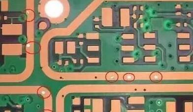
During wave soldering, reflow soldering, or other assembly processes, open vias can allow molten solder to flow through the hole.
This may result in:
- Solder loss from the intended joint
- Solder balls or solder accumulation on the opposite side
- Electrical shorts
- Insufficient solder joints
- Contamination around the assembly area
Proper Via Hole Plugging helps reduce these risks.
For via-in-pad structures used with BGA components, the plugging and planarization process is particularly important because an uneven or open via can interfere with solder deposition and BGA joint formation.
2. Reduce Flux and Contamination Trapped Inside the Hole
Open vias can collect flux residues, cleaning chemicals, moisture, dust, and other contaminants.
If the board is difficult to clean after assembly, contaminants trapped inside the via can potentially affect reliability. Plugging the hole reduces the exposed internal cavity and makes contamination control easier.
3. Improve Surface Flatness
BGA, CSP, QFN, and other fine-pitch packages require controlled pad geometry.
When a via is located in or near a solder pad, an open hole or excessive depression can affect solder paste deposition. A properly filled and planarized via creates a more uniform surface for SMT Assembly.
This is one reason why via filling and planarization are commonly considered for advanced BGA designs.
4. Prevent Solder Paste From Flowing Into the Hole
During stencil printing, solder paste can enter an exposed via.
This can reduce the amount of solder available on the pad and may contribute to poor solder joint formation. In fine-pitch assembly, even a small variation in solder volume can affect process yield.
Proper via plugging therefore helps maintain more predictable solder paste deposition.
5. Reduce Solder Ball and Short-Circuit Risks
During soldering, solder trapped inside or around an open via can move unexpectedly. Under certain process conditions, it may contribute to solder ball formation or electrical bridging.
For high-density BGA PCB designs, controlling the relationship between pads and vias is particularly important.
Main PCB Via Hole Plugging Processes
There is no single universal plugging process suitable for every PCB. The appropriate method depends on the hole diameter, board construction, copper thickness, solder mask system, surface finish, assembly requirements, and manufacturer’s equipment.
Several process approaches are commonly used.
1. Plugging After Hot Air Solder Leveling
One traditional approach is to perform solder mask plugging after hot air solder leveling (HASL).
A simplified process sequence is:
Solder Mask → HASL → Via Plugging → Curing
After the HASL process, selected holes can be plugged using a suitable solder mask or plugging ink. Screen printing or dedicated plugging equipment may be used depending on the production requirements.
Advantages
- Relatively straightforward process flow
- Can be used with different plugging materials
- Suitable for certain conventional PCB structures
- Does not require specialized via-filling equipment in some applications
Limitations
The main limitation is that HASL produces a relatively uneven surface compared with planar surface finishes. If the board requires high surface flatness, especially around BGA pads, this approach may not provide the required geometry.
Additional risks may include:
- Plugging ink contamination on the copper surface
- Uneven plugging
- Reduced pad flatness
- Difficulty controlling ink thickness
- Potential solderability issues if ink reaches the pad
Therefore, this process should be evaluated carefully for fine-pitch SMT Assembly applications.
2. Aluminum Screen Plugging and Planarization
Another approach uses a specially prepared aluminum screen or stencil to selectively plug the required holes.
The general process may include:
Pre-Treatment → Hole Plugging → Curing → Planarization/Grinding → Pattern Transfer → Etching → Surface Solder Mask
The aluminum tooling is prepared with openings corresponding to the holes that require plugging. Plugging ink is then forced into the holes under controlled pressure.
After curing, the surface may be planarized to remove excess resin or ink.
Advantages
This process can provide relatively good control of the plugging area and surface condition. With suitable materials and process parameters, it can produce a flatter plugged-hole surface than some conventional approaches.
Key Manufacturing Requirements
The process requires careful control of:
- Plugging ink viscosity
- Hole diameter
- Plugging pressure
- Curing temperature and time
- Copper thickness
- Grinding or planarization parameters
- Surface cleanliness
If excessive resin remains on the copper surface, subsequent imaging, plating, or solder mask processes may be affected.
For this reason, PCB Quality Control is particularly important during this process.
3. Plugging Through Screen Printing Before Surface Solder Mask
In another process configuration, holes are first plugged using a dedicated screen, followed by solder mask printing on the PCB surface.
A typical sequence is:
Pre-Treatment → Hole Plugging → Pre-Cure → Exposure/Development → Final Cure → Surface Solder Mask
This approach can provide good coverage when the screen, ink, pressure, and curing conditions are properly controlled.
Advantages
- Good compatibility with selective hole plugging
- Can achieve relatively consistent plugging
- Suitable for certain high-density PCB structures
- Can provide improved control of surface appearance
Potential Problems
Improper process parameters may result in:
- Ink entering areas where it is not required
- Voids inside the plugged hole
- Ink residue on solder pads
- Poor adhesion
- Blistering after thermal processing
- Reduced solderability
Therefore, process engineers must optimize screen tension, ink rheology, printing pressure, squeegee speed, curing conditions, and other parameters.
4. Simultaneous Solder Mask Printing and Hole Plugging
Some PCB processes use screen printing to perform surface solder mask coating and hole plugging within a coordinated process.
A simplified sequence is:
Pre-Treatment → Screen Printing → Pre-Cure → Exposure → Development → Final Cure
The objective is to cover the PCB surface while also preventing selected vias or holes from remaining open.
Advantages
- Shorter process flow
- Efficient equipment utilization
- Suitable for certain conventional PCB designs
- Can provide consistent solder mask appearance when properly controlled
Main Challenges
One major challenge is air trapped inside the hole during printing.
When the trapped air expands during curing or subsequent thermal processing, it may create:
- Voids
- Bubbles
- Local blistering
- Incomplete plugging
- Uneven solder mask coverage
These defects can become more noticeable during subsequent thermal processes such as reflow or HASL.
Therefore, the printing pressure, ink viscosity, screen parameters, hole geometry, and curing profile must be carefully controlled.
Via Plugging for BGA and Via-in-Pad Applications
BGA components place particularly high demands on PCB surface flatness.
When a via is positioned directly inside a BGA pad, an open via can allow solder paste to flow into the hole. This can change the solder volume available for the joint and potentially cause assembly defects.
For this reason, BGA PCB designs may use one of several approaches, including:
- Solder mask plugging
- Resin filling
- Via filling and planarization
- Filled and capped via structures
- Alternative pad/via arrangements
The appropriate method depends on the via structure, pad size, component pitch, board thickness, fabrication capability, and assembly process.
It is important to distinguish simple solder mask plugging from advanced via filling. A conventional plugged via may not provide the same degree of planarization as a filled-and-capped via.
For high-density BGA applications, the designer and manufacturer should confirm the required structure before PCB fabrication begins.
Materials Used for Via Plugging
The plugging material must be compatible with the PCB manufacturing process and subsequent assembly conditions.
Important material properties include:
Viscosity
The ink must be capable of entering the target hole without excessive spreading onto adjacent pads or copper areas.
Adhesion
Strong adhesion to the hole wall and surrounding material helps prevent cracking, peeling, or delamination during thermal cycling.
Low Shrinkage
Excessive shrinkage during curing can create internal voids or recesses.
Thermal Stability
The material must withstand subsequent processes such as solder mask curing, HASL where applicable, reflow soldering, and other thermal operations.
Electrical Properties
Depending on the application, the plugging material may need suitable dielectric properties and insulation performance.
Surface Compatibility
The material should not negatively affect subsequent solder mask, surface finish, solderability, or inspection processes.
Common Defects in PCB Hole Plugging
Although Via Hole Plugging improves PCB manufacturability and assembly reliability, poor process control can create new defects.
1. Incomplete Plugging
The hole is not completely filled, leaving an internal cavity.
This may allow flux or solder to enter the remaining space.
2. Excessive Plugging Ink
Too much ink can form a raised surface and interfere with pad flatness or subsequent surface processing.
3. Voids
Air or solvent trapped inside the plugging material can create internal voids.
4. Blistering
Poor curing, contamination, excessive moisture, or thermal stress may cause the plugging material to blister during later processing.
5. Cracking
Differences in thermal expansion between the plugging material, copper, and PCB dielectric can contribute to cracking under thermal stress.
6. Ink on Solder Pads
If plugging ink spreads onto the pad, it can reduce solderability and cause assembly defects.
7. Poor Adhesion
Insufficient surface preparation or incompatible materials may result in peeling or separation from the hole wall.
PCB Surface Finish and Hole Plugging
Hole plugging should also be considered together with the PCB Surface Finish.
Common PCB surface finishes include:
- HASL
- Lead-Free HASL
- ENIG
- Immersion Tin
- OSP
- Other application-specific finishes
The plugging process and surface finish cannot always be selected independently.
For example, BGA applications typically place greater emphasis on surface flatness, making planar surface finishes and controlled via structures particularly important.
In contrast, conventional through-hole or mixed-technology boards may have different requirements.
The final combination should be selected according to component package, soldering method, reliability requirements, cost targets, and manufacturing capability.
Design Guidelines for PCB Via Plugging
Good results begin at the PCB design stage.
Designers should consider:
1. Identify Which Vias Need Plugging
Not every via needs to be plugged. Plugging should be determined by electrical, mechanical, assembly, and reliability requirements.
2. Consider Via-in-Pad Requirements Early
If vias are located directly inside BGA or fine-pitch pads, the required plugging, filling, and planarization structure should be defined before manufacturing.
3. Maintain Adequate Pad Geometry
The pad size, via diameter, annular ring, and solder mask opening should be coordinated to prevent manufacturing and assembly problems.
4. Consider Surface Flatness
Fine-pitch packages are sensitive to variations in solder volume and pad geometry. Flatness should therefore be considered during both PCB design and fabrication.
5. Review the Design With the Manufacturer
Different PCB manufacturers have different screen-printing, via-filling, drilling, plating, curing, and planarization capabilities.
Early DFM communication can help avoid designs that are technically possible but difficult to manufacture consistently.
Quality Control for Via Plugging
Reliable PCB Manufacturing requires inspection at multiple stages.
Typical quality-control activities may include:
- Visual inspection
- Plugging coverage inspection
- Surface flatness inspection
- Cross-section analysis
- Microsection inspection
- Solderability testing
- Thermal stress testing
- Electrical testing
- Adhesion evaluation
- Process parameter monitoring
For critical BGA structures, cross-sectional analysis can help verify whether the hole is properly filled and whether voids, cracks, or separation exist.
Process capability should also be monitored rather than relying only on final inspection.
How Kingda Controls the Via Plugging Process
At Kingda, PCB Manufacturing is managed as an integrated process rather than treating hole plugging as an isolated operation.
For boards requiring Via Hole Plugging, Kingda evaluates the relationship between PCB design, drilling, copper plating, solder mask, surface finish, and assembly requirements.
Particular attention can be given to:
- Hole diameter and aspect ratio
- Via structure
- Copper thickness
- Plugging material selection
- Screen-printing parameters
- Curing conditions
- Surface flatness
- BGA and fine-pitch pad structures
- Surface finish compatibility
- PCB Quality Control
- Final SMT Assembly requirements
For high-density and BGA designs, early engineering communication helps determine whether conventional solder mask plugging, resin filling, or a more advanced filled-and-capped via structure is appropriate.
Conclusion
As electronic products continue to move toward higher density and smaller package sizes, Via Hole Plugging has become an important technology for many advanced PCB applications.
Proper hole plugging can prevent solder and flux from entering vias, improve pad flatness, support reliable BGA soldering, and reduce assembly-related defects. However, different PCB structures require different plugging processes, and no single method is suitable for every application.
The best results depend on coordinated control of PCB design, drilling, copper plating, plugging material, screen printing, curing, surface finish, inspection, and SMT Assembly.
For demanding applications such as HDI, fine-pitch, BGA, and high-density PCBs, selecting the appropriate hole-plugging structure at the design stage can significantly improve manufacturability and product reliability. Kingda can work with customers to evaluate these requirements and develop a practical manufacturing solution based on the actual PCB structure and assembly process.