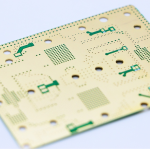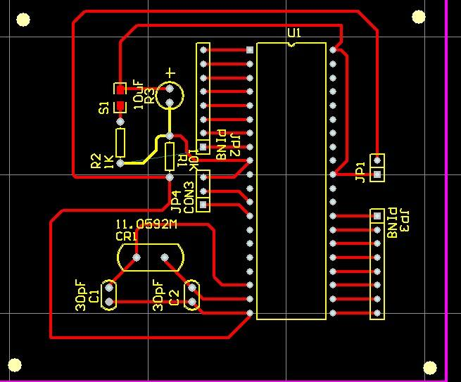
Modern electronic devices are developing toward higher operating speeds, lower power consumption, smaller form factors, and stronger immunity to electromagnetic interference. These trends place increasingly demanding requirements on High-Frequency PCB Design.
As signal edge rates become faster and interconnects become electrically longer, PCB routing can no longer be treated simply as a matter of connecting components. Trace geometry, reference planes, vias, return-current paths, crosstalk, grounding, and stackup all influence electrical performance.
Early PCB design software such as Protel provided designers with important tools for multilayer layout, automatic routing, copper pouring, and design-rule management. Although modern PCB design platforms have evolved considerably, many of the fundamental principles used for high-frequency routing remain relevant.
This article introduces practical PCB Routing strategies for high-frequency circuits and explains how layout, routing, grounding, and copper planes can be coordinated to improve Signal Integrity and reduce unwanted coupling.
1. Why High-Frequency PCB Routing Requires Special Attention
A high-frequency or high-speed PCB typically contains dense component placement, fast signal transitions, power distribution networks, and multiple signal layers.
Under these conditions, the PCB itself becomes part of the electrical system.
Important factors include:
- Trace impedance
- Return-current paths
- Signal propagation delay
- Crosstalk
- Via discontinuities
- Reference-plane continuity
- Grounding
- Power integrity
- Electromagnetic coupling
- Stackup geometry
The higher the signal bandwidth and the faster the rise/fall time, the more important these factors become.
It is therefore more appropriate to think of a high-speed trace as a transmission-line structure consisting of a signal conductor and its associated return path, rather than simply a piece of copper connecting two pins.
2. Multilayer PCB Design for High-Frequency Circuits
High-density high-frequency designs often benefit from multilayer PCBs because additional layers can provide dedicated signal, power, and reference-plane structures.
A properly designed multilayer stackup can provide:
- Shorter signal paths
- Better reference-plane continuity
- More controlled impedance
- Improved power distribution
- Reduced loop area
- Better electromagnetic isolation
- Greater routing density
However, adding more layers does not automatically improve performance.
A higher layer count also increases:
- Manufacturing complexity
- Lamination requirements
- Registration challenges
- Manufacturing cost
- Stackup-design complexity
The goal should therefore be to select a stackup that provides the required electrical performance while remaining practical to manufacture.
For High-Frequency PCB Design, signal layers should generally be positioned close to appropriate reference planes when controlled impedance and predictable return paths are required.
3. Keep High-Frequency Signal Paths Short
One of the most important principles in PCB Routing is to minimize unnecessary signal-path length.
Longer traces can increase:
- Propagation delay
- Insertion loss
- Parasitic capacitance
- Parasitic inductance
- Exposure to electromagnetic coupling
For high-speed interfaces, unnecessary detours should be avoided.
Component placement should therefore be planned before routing begins.
Critical components should be positioned so that high-speed connections can be routed directly and with minimal discontinuities.
For example, the signal path between a driver, connector, and receiver should be considered as a complete channel rather than routing each component independently.
4. Avoid Unnecessary Trace Bends
The original principle that high-frequency traces should avoid excessive bending remains useful, but the reason should be explained more precisely.
A 90-degree corner is not automatically a major high-frequency failure point. However, sharp corners can change local trace geometry and may introduce small impedance discontinuities.
For controlled-impedance and high-speed signals, smoother routing is generally preferred.
Modern PCB design tools commonly support:
- 45-degree routing
- Arc routing
- Curved corners
- Differential-pair routing
- Interactive impedance-aware routing
When routing critical signals, designers should prioritize:
- Continuous reference planes
- Controlled trace geometry
- Minimal unnecessary length
- Consistent spacing
- Smooth transitions
The exact routing strategy should be based on signal speed, rise time, stackup, and manufacturing capability.
5. Reduce Unnecessary Vias
Vias provide essential connections between PCB layers, but every via introduces parasitic effects.
A via can contribute:
- Parasitic capacitance
- Parasitic inductance
- Impedance discontinuity
- Via stub
- Additional signal-path length
Therefore, critical high-speed signals should use only the number of vias necessary to achieve the required routing structure.
This does not mean that vias should never be used.
Instead, the designer should evaluate whether each via creates a meaningful electrical discontinuity.
For very high-speed interfaces, techniques such as:
- Blind vias
- Microvias
- Back-drilling
- Via optimization
- Via-in-pad structures
may be considered where appropriate.
The correct approach depends on the interface, stackup, board thickness, manufacturing process, and cost target.
6. Control Crosstalk Between Parallel Traces
Crosstalk is one of the most important concerns in high-frequency PCB routing.
When two traces run close to each other, electromagnetic fields around the aggressor trace can couple energy into the neighboring victim trace.
This coupling has both capacitive and inductive components.
Capacitive coupling is related to changing voltage:
i = C × dv/dt
Inductive coupling is related to changing current:
V = M × di/dt
Therefore, fast signal transitions can generate significant coupling even when the nominal operating frequency does not appear particularly high.
Common methods for reducing crosstalk include:
- Increase spacing between sensitive traces.
- Reduce unnecessary parallel routing.
- Keep critical traces short.
- Use an appropriate reference plane.
- Route adjacent layers with suitable directional separation where practical.
- Use ground shielding structures where justified.
- Avoid routing high-noise and low-level analog signals together.
7. Use Adjacent-Layer Routing Carefully
A common PCB layout strategy is to route adjacent signal layers in different directions.
For example:
- Layer A: predominantly horizontal
- Layer B: predominantly vertical
This can reduce the length over which traces on adjacent layers run in parallel.
However, routing direction alone does not guarantee low Crosstalk.
The actual coupling also depends on:
- Layer spacing
- Trace width
- Trace spacing
- Dielectric properties
- Reference-plane structure
- Parallel-run length
- Signal rise time
Therefore, stackup and geometry should be considered together.
For demanding interfaces, field-solver calculations or electromagnetic simulation can provide more accurate coupling estimates than simple routing rules.
8. Maintain a Continuous Ground Plane
A continuous Ground Plane can provide a low-impedance return-current path and help reduce loop area.
For high-speed signals, the return current tends to follow the path of lowest impedance, which is strongly influenced by the reference plane and signal geometry.
If a signal crosses a gap or split in its reference plane, the return current may be forced to take a longer path.
This can increase:
- Loop area
- Electromagnetic radiation
- EMI susceptibility
- Signal discontinuity
- Crosstalk
Therefore, maintaining reference-plane continuity is one of the most important principles in PCB Grounding and high-speed layout.
9. Grounding Is More Than Simply Adding Copper
Adding a large amount of copper does not automatically produce a good grounding system.
Effective PCB Grounding requires careful consideration of current paths.
A good grounding strategy should address:
- Signal return paths
- Power return paths
- High-current switching loops
- Analog-sensitive circuits
- Digital switching circuits
- Connector interfaces
- Shield connections
- Chassis connections
The goal is to prevent high-current or high-frequency return currents from flowing through sensitive circuit regions.
For mixed-signal boards, simply splitting the ground plane into separate analog and digital sections is not always the best solution. The correct strategy depends on the circuit architecture and return-current behavior.
10. Copper Pour and Ground Planes
Copper pours can provide several benefits when properly implemented.
A large copper area connected to an appropriate ground network can:
- Reduce return-path impedance
- Reduce loop area
- Improve grounding
- Provide thermal spreading
- Increase copper distribution
- Improve mechanical robustness in some designs
In older PCB design workflows, polygon or copper-pour functions were used to create large ground areas around routed traces.
Modern PCB tools provide much more advanced control over copper pours, including:
- Clearance management
- Thermal relief
- Pour priorities
- Dynamic repouring
- Net assignments
- Keep-out regions
- Layer-specific rules
However, copper should not simply be poured everywhere.
Designers must ensure that copper does not unintentionally create:
- Floating conductive islands
- Uncontrolled capacitive coupling
- Inappropriate antenna structures
- Clearance violations
- Thermal-relief problems
- Unwanted connections between different electrical domains
11. Ground Vias for High-Frequency PCB Design
Ground vias can help connect a signal’s reference plane and reduce the impedance of return paths between layers.
For high-frequency structures, strategically placed ground vias can be used to:
- Connect adjacent ground planes
- Reduce return-path discontinuities
- Improve shielding
- Reduce loop area
- Support via fences
- Connect shielding structures to ground
A via fence may be useful around selected RF or sensitive circuit regions, but it should be designed according to wavelength, geometry, enclosure structure, and manufacturing capability.
There is no universal via spacing that works for every high-frequency design.
12. Separate Noisy and Sensitive Circuits
High-frequency PCB design should consider the source, coupling path, and victim.
Typical noise sources include:
- Switching regulators
- High-speed clocks
- Digital processors
- High-current switching devices
- RF transmitters
- Fast interfaces
Potential victims include:
- Analog amplifiers
- ADCs and DACs
- Sensors
- Low-level audio circuits
- RF receivers
- Precision measurement circuits
The placement strategy should prevent high-noise circuits from being physically and electrically coupled to sensitive circuits.
For example, a switching regulator should generally not be placed immediately next to a sensitive analog input simply because doing so produces a short routing distance.
Short routing is important, but signal integrity and electromagnetic isolation must be considered together.
13. Component Placement Before Routing
Good PCB Layout begins with component placement.
Before routing, designers should identify:
- High-speed interfaces
- Clock sources
- Differential pairs
- Power converters
- Analog signal paths
- RF circuits
- Connectors
- Sensitive measurement nodes
Critical components should then be arranged according to signal-flow direction.
A useful approach is to establish functional zones such as:
Power → Processing → High-Speed Interface → Connector
while keeping sensitive analog and RF sections appropriately isolated from noisy power and digital circuits.
This approach reduces unnecessary trace length and makes return-current management easier.
14. Differential Pair Routing
Many modern high-speed interfaces use differential signaling.
Examples include:
- USB
- PCI Express
- Ethernet
- Display interfaces
- LVDS
- High-speed ADC/DAC interfaces
Differential pairs should be routed according to the interface specification and the PCB stackup.
Important considerations include:
- Differential impedance
- Pair spacing
- Trace width
- Length matching
- Intra-pair skew
- Reference-plane continuity
- Via symmetry
- Connector transitions
It is not sufficient to simply keep two traces close together.
The differential pair must maintain appropriate coupling and impedance throughout the complete channel.
15. Controlled Impedance in High-Frequency PCB Routing
High-Frequency PCB traces may need controlled impedance when they operate as transmission lines.
Impedance depends on factors such as:
- Trace width
- Copper thickness
- Dielectric thickness
- Dielectric constant
- Trace-to-plane spacing
- Trace geometry
- Solder mask
- Differential-pair geometry
Therefore, impedance should be established from the actual PCB stackup rather than from a generic trace-width table.
For demanding designs, the manufacturer should provide a stackup and impedance calculation before production.
Kingda can work with customers to coordinate:
- Stackup selection
- Impedance targets
- Trace geometry
- Material selection
- Manufacturing tolerances
- Impedance testing
This helps bridge the gap between theoretical PCB design and actual manufacturing results.
16. Automatic Routing: Useful but Not a Substitute for Engineering
Automatic routing can significantly improve design efficiency, especially for complex boards.
However, fully automatic routing should not be blindly applied to critical high-frequency nets.
Important signals may require manually controlled routing to ensure:
- Correct topology
- Appropriate return paths
- Controlled spacing
- Proper differential-pair geometry
- Minimal vias
- Consistent impedance
- Reduced crosstalk
Automatic routing is most effective when combined with well-defined design constraints.
Modern PCB software allows designers to establish rules for:
- Trace width
- Clearance
- Differential pairs
- Impedance
- Layer usage
- Via structures
- Length matching
- High-speed nets
Constraint-driven routing can greatly improve consistency.
17. Protel and the Evolution of PCB Design Tools
Early versions of Protel introduced many useful PCB layout functions, including:
- Multilayer board design
- Automatic routing
- Copper pours
- Design-rule management
- Component placement
- Netlist-based design
These capabilities helped designers manage increasingly complex circuit boards.
Today, PCB design software has evolved to support much more advanced workflows, including:
- High-speed constraint management
- Differential-pair routing
- Length matching
- Impedance-aware design
- 3D mechanical integration
- Signal-integrity analysis
- Power-integrity analysis
- Thermal analysis
- Manufacturing-rule checking
The software itself is only one part of the solution.
A well-designed high-frequency PCB still depends on engineering knowledge, correct stackup design, appropriate materials, manufacturing capability, and verification.
18. Common High-Frequency PCB Routing Mistakes
Several common mistakes can reduce high-frequency PCB performance.
Mistake 1: Routing only according to the shortest distance
The shortest route is not always the best route if it crosses a poor reference-plane region or creates excessive coupling.
Mistake 2: Ignoring return current
A signal trace cannot be analyzed independently from its return path.
Mistake 3: Excessive parallel routing
Long parallel runs can increase capacitive and inductive coupling.
Mistake 4: Using too many vias
Unnecessary vias can create impedance discontinuities and additional parasitic effects.
Mistake 5: Treating copper pours as universal shielding
A copper pour is useful only when its electrical connection and geometry are appropriate.
Mistake 6: Splitting ground without analyzing return currents
An improperly placed ground split can force high-frequency return currents around the split and increase EMI.
Mistake 7: Relying only on automatic routing
Critical high-speed nets often require manually controlled routing and engineering constraints.
19. A Practical High-Frequency PCB Routing Workflow
A reliable PCB Routing workflow can be organized into the following steps:
Step 1: Identify Critical Nets
Classify high-speed, high-current, RF, clock, analog, and sensitive signals.
Step 2: Define the Stackup
Determine signal layers, reference planes, power layers, dielectric thickness, and target impedance.
Step 3: Place Components
Minimize critical signal paths and separate major noise sources from sensitive circuits.
Step 4: Establish Ground and Power Structures
Create stable return-current paths before routing critical signals.
Step 5: Route Critical Nets First
Prioritize differential pairs, clocks, high-speed buses, and other sensitive interfaces.
Step 6: Control Crosstalk
Review trace spacing, parallel-run length, layer arrangement, and reference-plane continuity.
Step 7: Optimize Vias
Reduce unnecessary transitions and manage via stubs and return-path continuity.
Step 8: Complete General Routing
Route lower-priority signals after critical networks have been established.
Step 9: Perform DRC and SI Review
Check electrical and manufacturing constraints.
Step 10: Verify With Simulation and Measurement
For demanding designs, use pre-layout/post-layout simulation and prototype measurements where appropriate.
20. How Kingda Supports High-Frequency PCB Manufacturing
Successful High-Frequency PCB Design requires close coordination between design and manufacturing.
Kingda can support customers with manufacturing considerations such as:
- Multilayer stackup planning
- Controlled impedance
- High-frequency material selection
- Fine-line fabrication
- Via and microvia structures
- Copper thickness control
- Registration accuracy
- Surface finish
- Electrical testing
- Manufacturing DFM review
The actual manufacturing capability should always be evaluated against the specific board structure and required tolerances.
For high-frequency products, even relatively small manufacturing variations can affect impedance and signal performance.
Therefore, PCB designers and manufacturers should establish critical parameters before production rather than discovering limitations after fabrication.
21. High-Frequency PCB Routing Checklist
Before releasing a high-frequency PCB for manufacturing, review the following:
-
Is the PCB stackup appropriate for the signal requirements?
-
Are critical signals routed over continuous reference planes?
-
Are differential pairs routed according to their impedance requirements?
-
Are unnecessary vias minimized?
-
Are via stubs properly evaluated?
-
Is crosstalk controlled through spacing and routing strategy?
-
Are high-noise and sensitive circuits appropriately separated?
-
Are return-current paths continuous?
-
Are ground vias used where they provide a meaningful electrical benefit?
-
Are copper pours correctly connected?
-
Are impedance requirements documented?
-
Has the manufacturer confirmed the required tolerances?
-
Has DRC been completed?
-
Has signal-integrity simulation been considered for critical interfaces?
-
Have prototype measurements been planned where necessary?
Conclusion
As electronic systems continue to move toward higher speeds, smaller form factors, and greater integration, High-Frequency PCB Design requires much more than simply connecting components with copper traces.
Effective PCB Routing should consider the complete electrical structure, including signal paths, return-current paths, reference planes, vias, impedance, component placement, and Crosstalk.
The most important principles are:
- Keep critical signal paths appropriately short.
- Maintain continuous reference planes.
- Minimize unnecessary vias and discontinuities.
- Control trace spacing and parallel routing.
- Use appropriate grounding strategies.
- Separate noise sources from sensitive circuits.
- Establish controlled impedance from the actual stackup.
- Use automatic routing together with engineering constraints.
- Verify critical designs through simulation and measurement.
- Coordinate PCB design requirements with manufacturing capabilities.
Although PCB design software has evolved significantly since the early Protel era, the fundamental objective remains the same: create a predictable electrical environment in which high-speed signals can propagate reliably.
With appropriate PCB Layout, PCB Grounding, stackup design, routing control, and manufacturing coordination, Kingda can help customers develop reliable high-frequency and high-speed PCBs for demanding electronic applications.