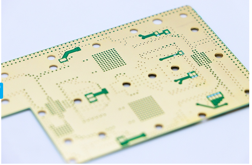
As electronic products continue to become smaller, faster, and more highly integrated, the requirements for PCB manufacturing technology are also becoming increasingly demanding. Among the many processes involved in PCB production, PCB Surface Finish is particularly important because it directly affects solderability, copper protection, contact reliability, storage life, and assembly performance.
The copper exposed on a finished PCB is vulnerable to oxidation and contamination. Without appropriate protection, the copper surface can deteriorate during storage and may no longer provide the surface condition required for reliable soldering or electrical contact.
This is why manufacturers apply different types of Surface Treatment to exposed copper areas.
Common options include:
- HASL
- Lead-Free HASL
- ENIG
- Immersion Tin
- Immersion Silver
- OSP
- Electroplated Gold
- Hard Gold
Each finish has different characteristics. There is no single surface finish that is ideal for every PCB application.
For this reason, selecting the right PCB Surface Finish requires consideration of PCB design, component pitch, soldering process, contact requirements, storage conditions, cost, and reliability requirements.
1. Why PCB Surface Finish Is Important
Copper is an excellent electrical conductor and is widely used as the conductor material in PCBs. However, exposed copper reacts with oxygen and other environmental contaminants.
Oxidized copper can have a negative effect on:
- Solderability
- Electrical contact
- Surface appearance
- Long-term storage
- Plating adhesion
- Assembly yield
A suitable Surface Treatment protects the exposed copper and creates a more appropriate interface for soldering or electrical contact.
The main functions of a PCB Surface Finish include:
- Protecting exposed copper from oxidation.
- Maintaining solderability during PCB assembly.
- Providing a suitable contact surface where required.
- Improving storage stability.
- Supporting reliable SMT and through-hole assembly.
- Meeting application-specific electrical and mechanical requirements.
The best finish depends on how the PCB will be used.
2. Bare Copper: Low Cost but Limited Protection
Bare copper is the simplest PCB surface condition.
It offers several natural advantages:
- Low material cost
- Excellent electrical conductivity
- Good solderability when fresh
- Simple manufacturing process
However, exposed copper oxidizes relatively easily.
As oxidation progresses, the solderability of the surface can deteriorate. Therefore, bare copper is generally not suitable for applications requiring extended storage or long-term exposure before assembly.
For this reason, most commercial PCBs use a protective PCB Surface Finish rather than leaving important solderable copper areas completely exposed.
3. HASL: A Cost-Effective and Widely Used Surface Finish
HASL stands for Hot Air Solder Leveling.
During the HASL process, the PCB is coated with molten solder and then passed through hot-air knives to remove excess solder and produce a relatively uniform solder coating.
Traditional HASL uses lead-containing solder alloys, while lead-free HASL uses lead-free alloys.
Advantages of HASL
HASL is widely used because it offers:
- Good solderability
- Relatively low cost
- Mature manufacturing technology
- Good solder-joint compatibility
- Robust processing characteristics
Lead-free HASL is commonly selected when the product must meet applicable lead-restriction requirements.
Limitations of HASL
The main limitation is surface flatness.
Because the coating is created by molten solder leveling, the surface may not be as planar as immersion finishes. This can become important for:
- Fine-pitch components
- Small passive components
- BGA packages
- QFN packages
- High-density SMT assembly
Thermal exposure during HASL processing should also be considered when evaluating the complete PCB manufacturing process.
4. Lead-Free HASL
Lead-Free HASL is an alternative to traditional leaded HASL for products that require compliance with lead-restriction requirements.
Lead-free solder alloys generally have higher melting temperatures than conventional Sn-Pb solder, so the thermal profile of the process must be appropriately controlled.
Advantages
- Suitable for many lead-free assembly processes
- Good solderability
- Relatively economical
- Mature manufacturing process
- Suitable for many general-purpose PCB applications
Limitations
- Surface flatness is generally lower than ENIG
- Thermal exposure is relatively high
- May be less suitable for very fine-pitch components
Therefore, Lead-Free HASL remains a practical choice for many conventional PCB applications where cost and solderability are important.
5. ENIG: Excellent Flatness for Fine-Pitch PCB Assembly
ENIG stands for Electroless Nickel Immersion Gold.
It consists primarily of:
- An electroless nickel layer deposited over the copper.
- A thin immersion gold layer deposited over the nickel.
ENIG is one of the most widely used PCB Surface Finish options for modern high-density electronic products.
Advantages of ENIG
ENIG provides:
- Excellent surface flatness
- Good solderability
- Good oxidation resistance
- Suitable performance for fine-pitch SMT
- Good compatibility with BGA and QFN assembly
- Good storage stability
- Suitable surface characteristics for many contact and assembly applications
Its flat surface makes ENIG particularly attractive for high-density PCB designs.
Limitations of ENIG
Compared with HASL, ENIG generally has higher processing cost.
The electroless nickel process also requires careful chemical control. Poor process control can contribute to defects such as excessive nickel corrosion or the phenomenon commonly referred to as black pad.
Therefore, ENIG quality depends strongly on bath chemistry, process control, coating thickness, and inspection.
6. Gold Plating: Different Processes for Different Applications
The term “gold-plated PCB” can refer to several different processes, and they should not be treated as interchangeable.
For example, immersion gold and electroplated gold have different structures and applications.
Immersion Gold
Immersion gold is normally used as the final protective layer over electroless nickel in ENIG.
The gold layer is relatively thin and primarily protects the underlying nickel surface and provides a suitable soldering interface.
It should not be confused with a thick gold contact surface.
Electroplated Gold
Electroplated gold can be used where the surface must withstand repeated mechanical contact.
Typical applications include:
- Gold fingers
- Edge connectors
- Switch contacts
- Connector contact areas
Hard gold is often selected for applications involving repeated mechanical contact because its properties can be engineered for greater wear resistance than a thin immersion-gold layer.
Therefore, Gold Plating should be selected according to whether the application requires solderability, corrosion protection, electrical contact, or mechanical wear resistance.
7. Gold Fingers and Contact Areas
Gold fingers are a common example of a PCB area that requires a specialized Surface Treatment.
These contact areas may be inserted into connectors repeatedly, so the surface needs to withstand mechanical wear while maintaining stable electrical contact.
For this reason, the requirements for gold fingers differ significantly from those of normal SMT solder pads.
Typical considerations include:
- Gold thickness
- Nickel thickness
- Hardness
- Wear resistance
- Contact reliability
- Edge geometry
- Connector compatibility
It is therefore incorrect to assume that all gold-colored PCB surfaces use the same manufacturing process.
The color of a PCB surface alone cannot reliably identify the specific finish.
8. OSP: A Thin Organic Protective Layer
OSP stands for Organic Solderability Preservative.
Unlike HASL or ENIG, OSP does not create a metallic coating over the copper. Instead, it forms a thin organic protective layer that helps prevent oxidation before soldering.
Advantages of OSP
OSP is attractive because it provides:
- Low cost
- Flat copper surfaces
- Good solderability when properly processed and stored
- Good suitability for fine-pitch SMT
- A relatively simple surface structure
- Lead-free compatibility
Because OSP does not significantly change the geometry of the copper pad, it can be useful for fine-pitch PCB assembly.
Limitations of OSP
OSP is more sensitive to handling, storage, contamination, and process conditions than some metallic finishes.
Its performance can also be affected by:
- Storage duration
- Temperature
- Humidity
- Packaging
- Handling contamination
- Multiple thermal cycles
- Assembly process conditions
Therefore, OSP should be evaluated according to the actual assembly and storage requirements rather than using a universal expiration period.
9. Immersion Tin and Immersion Silver
Other metallic PCB Surface Finish options include immersion tin and immersion silver.
Immersion Tin
Immersion tin provides a relatively flat surface and can offer good solderability.
It may be considered for fine-pitch PCB assembly where surface planarity is important.
However, storage, handling, whisker risk, surface contamination, and process control should be evaluated according to the specific application.
Immersion Silver
Immersion silver provides a flat surface and good solderability.
It can be used in applications where fine-pitch assembly and surface planarity are important.
However, silver surfaces require appropriate packaging and handling because contamination and environmental exposure can affect surface quality.
10. PCB Surface Finish Comparison
Different finishes provide different combinations of cost, flatness, solderability, contact performance, and storage stability.
| Surface Finish | Flatness | Solderability | Relative Cost | Typical Applications |
|---|---|---|---|---|
| Bare Copper | Excellent | Good when fresh | Low | Limited-use applications |
| HASL | Moderate | Good | Low | General PCB assembly |
| Lead-Free HASL | Moderate | Good | Low–Moderate | Lead-free products |
| ENIG | Excellent | Very Good | Moderate–High | Fine-pitch SMT, BGA, QFN |
| OSP | Excellent | Good | Low | Fine-pitch, cost-sensitive SMT |
| Immersion Tin | Excellent | Good | Moderate | Fine-pitch applications |
| Immersion Silver | Excellent | Good | Moderate | Fine-pitch and selected applications |
| Electroplated Gold | Excellent | Application-dependent | High | Contacts, gold fingers, wear areas |
The table provides a general comparison. Actual performance depends on material, process control, board design, assembly conditions, and customer specifications.
11. How to Choose the Right PCB Surface Finish
There is no universal best PCB Surface Finish.
The appropriate selection should be based on the complete product requirement.
Consider Component Pitch
If the PCB contains fine-pitch components, BGA, QFN, or other packages with demanding pad geometry, a relatively flat finish such as ENIG or OSP may be advantageous.
Consider Soldering Process
The finish must be compatible with the planned assembly process, including:
- SMT reflow
- Wave soldering
- Selective soldering
- Hand soldering
- Multiple reflow cycles
Consider Storage Requirements
If the PCB needs to be stored for an extended period before assembly, oxidation resistance and packaging requirements should be considered carefully.
Consider Contact Requirements
If a PCB includes connectors, edge contacts, or gold fingers, the required Gold Plating process may differ from the finish used on normal solder pads.
Consider Cost
For high-volume, cost-sensitive products, HASL or OSP may be attractive.
For fine-pitch or more demanding applications, ENIG or another suitable flat finish may provide better overall manufacturing value.
12. Surface Finish and PCB Solderability
One of the primary purposes of Surface Treatment is to maintain solderability.
However, solderability is not determined by the surface finish alone.
Other factors include:
- Copper surface condition
- Surface-finish quality
- Storage environment
- PCB cleanliness
- Solder paste properties
- Reflow profile
- Component condition
- Assembly handling
For example, a properly manufactured ENIG board can still experience soldering problems if the PCB has been contaminated or improperly stored.
Therefore, PCB Solderability should be controlled across the entire manufacturing and assembly chain.
13. Surface Finish and Fine-Pitch Components
As PCB designs become increasingly dense, surface flatness becomes more important.
Traditional HASL can create more surface variation because molten solder is leveled across the copper pads.
This may be acceptable for conventional components but can become less desirable for extremely fine-pitch devices.
Flat finishes such as ENIG and OSP can provide more uniform pad geometry.
However, surface flatness is only one part of the assembly equation. Pad design, stencil design, solder paste volume, component coplanarity, placement accuracy, and reflow control are also important.
14. Surface Finish and PCB Reliability
The choice of PCB Surface Finish can also affect long-term reliability.
Important factors include:
- Corrosion resistance
- Solder-joint integrity
- Thermal cycling
- Mechanical contact
- Storage conditions
- Chemical compatibility
- Plating adhesion
For high-reliability products, surface finish selection should be made together with material selection, PCB design, manufacturing process, and assembly requirements.
There is no universal finish that provides the highest reliability in every application.
15. Common Misunderstandings About PCB Surface Finishes
Myth 1: Gold-colored PCB means the entire board is plated with gold
Not necessarily.
A gold-colored surface may be associated with ENIG, electroplated gold, or another gold-containing finish. The process and layer structure must be verified from the manufacturing specification.
Myth 2: More gold always means better quality
Not necessarily.
The appropriate gold thickness and process depend on the intended application. Soldering pads, gold fingers, and mechanical contacts have different requirements.
Myth 3: HASL is always inferior
Not necessarily.
HASL is a mature and cost-effective finish with good solderability. It remains suitable for many conventional PCB applications.
Myth 4: OSP always has a fixed short usage period
Actual storage and assembly windows depend on the OSP chemistry, packaging, environmental conditions, handling, and customer requirements.
Myth 5: Surface finish alone determines PCB quality
PCB quality depends on the complete manufacturing system, including materials, drilling, imaging, etching, plating, solder mask, surface finish, testing, and process control.
16. How Kingda Controls PCB Surface Treatment
At Kingda, surface finishing is treated as an integral part of the overall PCB Manufacturing process.
The appropriate Surface Treatment is selected according to the PCB structure, assembly process, electrical requirements, mechanical requirements, storage conditions, and application environment.
Our manufacturing approach can include process control for:
- Copper surface preparation
- Solder mask processing
- HASL
- Lead-free HASL
- ENIG
- OSP
- Immersion finishes
- Electroplated gold
- Contact and gold-finger areas
- Surface-finish inspection
- Solderability evaluation
- Plating-thickness verification
For fine-line, HDI, multilayer, high-speed, flexible, and rigid-flex boards, the surface finish should be considered together with the overall PCB design and manufacturing process.
17. Final Checklist for Selecting a PCB Surface Finish
Before choosing a surface finish, ask the following questions:
- What type of components will be assembled?
- Are fine-pitch, BGA, or QFN packages used?
- Will the PCB undergo one or multiple reflow cycles?
- Does the product require long-term storage?
- Are there connector or gold-finger contact areas?
- Is the PCB exposed to humidity or corrosive environments?
- Is surface flatness critical?
- What level of PCB Solderability is required?
- What manufacturing cost target must be achieved?
- Are there environmental or compliance requirements?
Answering these questions will help determine the most appropriate PCB Surface Finish.
Conclusion
Different PCB surface finishes serve different purposes.
HASL provides a cost-effective solution with good solderability for many general applications. ENIG offers excellent flatness and is widely used for fine-pitch and high-density assembly. OSP provides a thin, flat, cost-effective protective layer for many SMT applications. Gold Plating is particularly important for selected contact and wear-resistant areas, while immersion tin and immersion silver provide additional options for specific applications.
The key is not to select a finish based simply on appearance or price.
Instead, consider:
- PCB design
- Component package
- Soldering process
- Storage conditions
- Electrical contact requirements
- Mechanical requirements
- Reliability expectations
- Manufacturing cost
- Applicable compliance requirements
With the right PCB Surface Finish and appropriate process control, manufacturers can improve PCB Solderability, protect exposed copper, support reliable assembly, and achieve more consistent long-term PCB performance.
Kingda can help customers evaluate surface-finish options according to their PCB structure, assembly requirements, and manufacturing objectives, supporting the transition from prototype development to stable production.