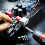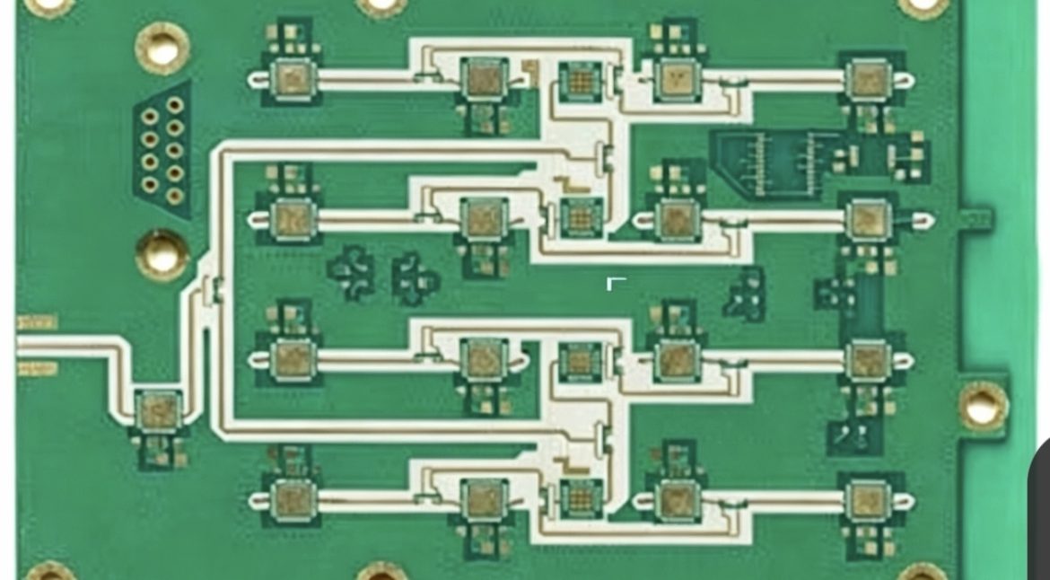
When repairing a printed circuit board, the first step should not be to power it on immediately. A careful Visual Inspection can often reveal obvious signs of damage and help prevent additional failures.
This is especially important when a PCB has been exposed to overvoltage, excessive current, overheating, short circuits, or component failure. If the board shows signs of burning or physical damage, the power and protection circuits should be checked carefully before applying power.
PCB Troubleshooting begins with understanding the board’s condition, identifying visible abnormalities, and then narrowing down the possible failure area through systematic testing.
Visual inspection is a static diagnostic method. Although it cannot identify every electrical fault, it is an efficient first step in Circuit Board Repair and can prevent unnecessary damage during subsequent testing.
1. Check the PCB for Mechanical or Human-Induced Damage
The first stage of PCB Repair is to determine whether the board has suffered physical damage during transportation, installation, operation, or previous maintenance.
Carefully inspect the PCB from both sides and check for the following conditions:
PCB Edge and Corner Damage
If a PCB has been dropped or subjected to mechanical stress, its corners or edges may be cracked, deformed, or broken.
Check whether:
- The PCB edge is cracked or chipped.
- Board corners are deformed.
- Mounting holes are damaged.
- Copper traces near the board edge are broken.
- Components close to the damaged area have been displaced.
Mechanical damage can sometimes produce intermittent faults that are difficult to identify during normal electrical testing.
IC Socket and Connector Damage
If the board contains IC sockets, connectors, or removable components, inspect them carefully.
A socket may be damaged if excessive force or an inappropriate tool was used during removal. Bent connector pins can also cause open circuits or unintended connections.
During Circuit Board Repair, mechanical damage should be distinguished from electrical failure because replacing an electronic component will not solve a problem caused by a damaged connector or PCB structure.
Incorrect IC Installation
For boards containing socketed integrated circuits, verify that each device is installed in the correct position and orientation.
Check:
- IC reference designators.
- Pin-1 orientation.
- Socket orientation.
- Device type and package.
- Bent or missing pins.
- Evidence of reversed insertion.
Installing an IC in the wrong orientation can cause excessive current consumption or immediate component failure when power is applied.
This is one reason why Visual Inspection should be completed before applying power to a damaged PCB.
Incorrect Jumper or Shorting Link Position
Some PCBs use jumpers, configuration links, or shorting terminals to select different operating modes.
Check whether:
- A jumper is installed in the correct position.
- The jumper configuration matches the schematic or assembly documentation.
- A shorting link has accidentally created an unintended connection.
- Configuration pins have been damaged.
A simple configuration error can sometimes appear to be a more serious hardware failure.
2. Inspect PCB Components for Signs of Burning or Physical Damage
The next step in PCB Failure Analysis is to inspect individual components.
Look carefully for:
- Burn marks.
- Discoloration.
- Cracked packages.
- Bulging capacitors.
- Melted plastic packages.
- Broken leads.
- Damaged solder joints.
- Carbonized PCB material.
- Unusual residue or contamination.
Common components that should receive particular attention include resistors, capacitors, diodes, transistors, voltage regulators, MOSFETs, and power-management devices.
Resistors
A visibly burned resistor may have changed value or become open-circuit. However, appearance alone cannot determine whether a resistor is electrically defective.
A resistor that looks normal may also have failed electrically.
Therefore, Multimeter Testing should be used when necessary to verify resistance and circuit continuity.
When measuring a resistor on a PCB, remember that parallel circuit paths can affect the measured value. For accurate diagnosis, the component may need to be isolated from the circuit.
Capacitors
Capacitors can fail through short circuits, open circuits, leakage, capacitance degradation, or increased equivalent series resistance (ESR).
Visible warning signs include:
- Bulging or venting.
- Cracked ceramic bodies.
- Burn marks.
- Discoloration.
- Damaged terminals.
A capacitor that looks normal is not necessarily electrically healthy, so additional measurements may be required.
Diodes and Semiconductor Devices
A damaged diode, MOSFET, transistor, or regulator may show obvious burn marks, cracks, or discoloration.
However, semiconductor failures are not always visible.
Using a multimeter’s diode-test function can provide useful information for many discrete semiconductor devices. For more complex components, additional circuit-level testing may be necessary.
3. Inspect ICs and Other Integrated Devices
Integrated circuits should also be examined carefully during PCB Troubleshooting.
Look for:
- Cracks in the IC package.
- Burn marks.
- Localized discoloration.
- Package deformation.
- Melted or damaged pins.
- Unusual soldering conditions.
- Signs of overheating around the device.
Older logic devices, processors, interface ICs, analog-to-digital converters, memory devices, and power-management ICs can all be potential failure points depending on the circuit architecture.
A visibly cracked or severely burned IC is strong evidence of physical damage, but visual evidence alone should not be treated as the only basis for replacement.
Some IC failures produce no visible external symptoms. In such cases, the repair process should continue with voltage measurements, continuity checks, signal measurements, or functional testing.
4. Check PCB Traces, Pads, Vias, and Copper Features
The PCB itself can fail even when all major components appear normal.
During Visual Inspection, examine:
- PCB traces.
- Solder pads.
- Via holes.
- Plated through-holes.
- Copper pours.
- Component footprints.
- Solder joints.
- Board edges.
Damaged or Lifted Traces
Excessive heat, mechanical stress, or previous rework can cause copper traces to lift from the substrate or become partially detached.
A damaged trace may create an intermittent open circuit that is difficult to detect without continuity testing.
Burned or Broken Traces
High current caused by a short circuit can overheat a PCB trace.
In severe cases, the copper may become discolored, lifted, or completely open.
When a burned trace is discovered, simply repairing the trace may not solve the problem. The technician should determine why the excessive current occurred before replacing or rebuilding the copper connection.
Via and Plated Through-Hole Inspection
Inspect vias and plated through-holes for:
- Cracks.
- Damaged pads.
- Poor solder joints.
- Mechanical damage.
- Signs of overheating.
- Abnormal plating conditions.
In multilayer PCBs, an internal connection may be damaged even when the external surface looks relatively normal. Electrical continuity testing and cross-sectional analysis may be required for difficult failures.
5. Check Fuses and Protection Components
Protection components should be inspected before powering a damaged PCB.
These may include:
- Fuses.
- Resettable fuses.
- Thermal fuses.
- TVS diodes.
- Overvoltage protection devices.
- Current-limiting components.
- Surge protection components.
If a fuse is open, do not assume that replacing the fuse will solve the problem.
A fuse usually opens because the circuit experienced excessive current or another abnormal condition. Replacing it without identifying the underlying cause may result in repeated failure or further PCB damage.
When the fuse element cannot be inspected visually, Multimeter Testing can be used to check continuity.
6. Use a Multimeter to Confirm Suspected Failures
Visual inspection is an important first step, but it cannot replace electrical testing.
After identifying suspicious areas, use a multimeter to perform appropriate measurements.
Typical checks include:
Continuity Testing
Continuity testing can help identify:
- Broken traces.
- Open connections.
- Damaged jumpers.
- Connector problems.
- Unexpected connections.
Resistance Measurement
Resistance measurements can help identify short circuits or abnormal resistance between power and ground.
However, an in-circuit resistance reading should be interpreted carefully because multiple components may be connected in parallel.
Diode Testing
The diode-test function can be useful for checking many discrete semiconductor devices.
Voltage Measurement
After confirming that it is safe to power the board, measure important supply rails and reference points.
Examples include:
- Input supply voltage.
- Main power rails.
- Regulator outputs.
- IC supply pins.
- Reference voltages.
- Ground connections.
The measured values should be compared with the schematic, datasheet, service documentation, or known-good board.
7. Trace the Failure Through the Schematic
Once visible damage has been identified, the next stage of PCB Failure Analysis is to understand the circuit around the suspected component.
A useful troubleshooting approach is:
Failed component → upstream circuit → power source → protection circuit → control circuit
For example, if a voltage regulator is burned, do not immediately replace it.
First determine:
- What voltage is supplied to the regulator?
- Is the input voltage within the expected range?
- Is there a short circuit on the regulator output?
- What components are connected to the output?
- Is the regulator controlled by another IC?
- Are protection components functioning correctly?
- Could an external load have caused the failure?
This systematic approach is much more effective than replacing components one by one.
8. Understand the Relationship Between Excessive Current and PCB Damage
Several visible PCB failures can be associated with excessive current, including burned resistors, damaged semiconductor devices, blown fuses, and burned traces.
However, excessive current is usually a symptom, not the complete root cause.
Possible causes include:
- Short circuits.
- Incorrect power supply.
- Reverse polarity.
- Failed semiconductor devices.
- Incorrect component installation.
- Damaged cables or connectors.
- Excessive load.
- Insulation breakdown.
- ESD or surge events.
- Power-supply instability.
- Thermal stress.
Therefore, good PCB Troubleshooting should always move from the visible symptom toward the electrical root cause.
9. Follow a Safe Power-Up Procedure
One of the most important principles in PCB Repair is avoiding unnecessary secondary damage.
A damaged PCB should not simply be connected to a normal power supply and switched on.
Before power-up:
- Inspect the PCB carefully.
- Check for obvious shorts.
- Verify the input polarity.
- Inspect protection components.
- Check the main power rail resistance where appropriate.
- Confirm critical components are installed correctly.
- Use a current-limited bench power supply when appropriate.
- Monitor current consumption during initial power-up.
- Measure important voltage rails.
- Stop immediately if abnormal current, smoke, excessive heating, or unusual noise occurs.
Current limiting can reduce the risk of turning a localized fault into widespread damage.
10. Common Mistakes During PCB Repair
Several common mistakes can make Circuit Board Repair more difficult.
Replacing a Fuse Without Finding the Cause
A blown fuse is often an indication of another failure. Replacing it without troubleshooting the circuit may result in another blown fuse.
Replacing a Burned Component Immediately
A burned component may be the result of another upstream or downstream fault.
The root cause should be investigated before the replacement component is installed.
Relying Only on Appearance
Not every defective component shows visible damage.
Electrical testing is necessary when the failure cannot be determined through Visual Inspection.
Powering the Board Too Early
Applying power before checking for shorts or incorrect connections can cause secondary damage.
Measuring Components Without Considering the Circuit
In-circuit measurements can be affected by other connected components. A measurement should therefore be interpreted according to the circuit topology.
11. A Systematic PCB Troubleshooting Workflow
For practical repair work, the following workflow can provide a reliable starting point:
Step 1: Collect the PCB schematic, BOM, layout files, or service documentation if available.
Step 2: Perform a complete Visual Inspection.
Step 3: Identify burned, cracked, displaced, missing, or incorrectly installed PCB Components.
Step 4: Inspect traces, pads, vias, connectors, and protection components.
Step 5: Perform continuity and resistance measurements with a multimeter.
Step 6: Identify the power path and locate possible short circuits.
Step 7: Analyze the circuit surrounding the suspected failure.
Step 8: Replace defective components only after investigating the probable cause.
Step 9: Power the board using appropriate current limiting and monitoring.
Step 10: Verify supply rails and key signals.
Step 11: Perform functional testing.
Step 12: Document the failure mechanism and repair result.
This approach combines visual evidence, electrical measurements, circuit analysis, and practical experience to improve PCB Failure Analysis.
12. How Kingda Supports PCB Reliability and Manufacturing
Reliable PCB Manufacturing can reduce the probability of defects that later become difficult repair problems. Manufacturing quality depends on material selection, PCB fabrication processes, plating quality, solder mask application, drilling, lamination, electrical testing, and final inspection.
For production PCBs, Kingda can support customers with PCB manufacturing and engineering coordination, helping evaluate design requirements, manufacturability, material selection, process control, and quality requirements.
When a board enters the repair or failure-analysis stage, manufacturing records and design documentation can also provide valuable information for identifying potential causes.
Conclusion
Effective PCB Troubleshooting should begin with observation rather than immediate power-up. A systematic Visual Inspection can reveal mechanical damage, burned components, incorrect installation, damaged traces, failed protection devices, and other obvious problems.
However, visual inspection is only the first stage of professional PCB Repair. Multimeter measurements, schematic analysis, controlled power-up, signal testing, and root-cause analysis are often required to identify hidden electrical failures.
By combining careful inspection with structured PCB Failure Analysis, engineers and technicians can reduce secondary damage, shorten troubleshooting time, and improve the reliability of Circuit Board Repair.