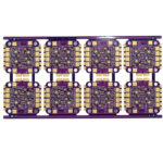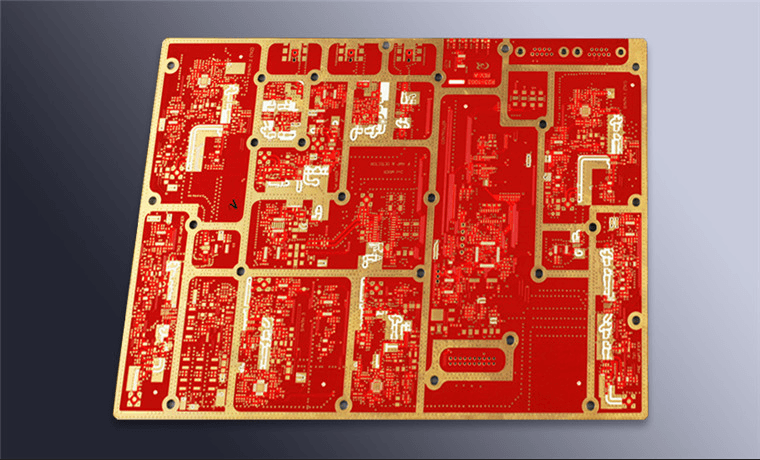
As electronic products become smaller, faster, and more highly integrated, conventional multilayer PCB structures may no longer provide sufficient routing density. HDI PCB technology addresses these challenges by using microvias, fine lines, fine-pitch interconnections, and sequential build-up structures to provide higher wiring density within a compact board area.
However, higher routing density also introduces stricter requirements for PCB layout, signal integrity, impedance control, power distribution, and manufacturing accuracy.
For high-speed and RF applications, engineers must consider not only whether a connection can be routed, but also how the routing structure affects signal quality and whether the design can be manufactured consistently.
The following guidelines summarize important considerations for HDI Routing, particularly when high-speed or high-frequency signals are involved.
1. Select Appropriate Materials for HDI PCB Design
Material selection is one of the foundations of reliable HDI PCB design.
For conventional digital circuits, standard FR-4 materials may be sufficient. However, high-speed and RF applications may require materials with tighter control of dielectric properties and loss characteristics.
Important material parameters include:
- Dielectric constant (Dk)
- Dissipation factor (Df)
- Glass transition temperature (Tg)
- Coefficient of thermal expansion (CTE)
- Thermal conductivity
- Copper surface roughness
- Resin content and dielectric thickness
- Moisture absorption
For a High-Frequency PCB, dielectric loss and conductor loss can become significant as frequency and data rates increase. The effective dielectric environment around a transmission line also affects its impedance and propagation characteristics.
Therefore, material selection should be based on the actual frequency range, signal rise time, stackup, thermal requirements, reliability requirements, and manufacturer capabilities rather than simply choosing a material with a high nominal performance rating.
2. Plan the HDI Stackup Before Routing
A well-defined stackup is essential for HDI Routing.
Before starting detailed routing, engineers should determine:
- Number of signal layers.
- Power and ground reference layers.
- Core and prepreg structures.
- Dielectric thickness.
- Copper thickness.
- Microvia structures.
- Controlled-impedance requirements.
- Sequential lamination strategy.
- Via transitions between layers.
For high-speed signals, maintaining a continuous and predictable reference plane is particularly important.
A carefully designed stackup helps control impedance, reduce discontinuities, and provide a predictable return-current path.
For complex HDI PCB designs, routing should therefore be performed only after the stackup and key manufacturing constraints have been established.
3. Keep High-Frequency Signal Paths Short and Direct
Short signal paths generally reduce parasitic effects and make high-speed routing easier to control.
During PCB Layout, avoid unnecessary:
- Trace length.
- Layer transitions.
- Vias.
- Stubs.
- Branches.
- Sharp changes in geometry.
- Uncontrolled reference-plane transitions.
For high-frequency signals, even a relatively small geometric discontinuity can affect insertion loss, reflection, or return-current behavior.
The objective is not simply to make every trace perfectly straight. Instead, routing should maintain consistent geometry and a continuous signal-return structure.
4. Use Microvias Correctly
Microvias are one of the most important technologies used in HDI PCB construction.
Compared with conventional through-hole vias, microvias can connect adjacent layers while consuming less routing area. This allows designers to escape fine-pitch packages and increase routing density.
Common HDI via structures include:
- Blind microvias.
- Stacked microvias.
- Staggered microvias.
- Buried vias.
- Through vias.
- Via-in-pad structures.
However, microvias should not be added simply because the board is classified as HDI.
Each via structure introduces electrical and manufacturing considerations. These can include parasitic capacitance and inductance, plating reliability, registration accuracy, thermal stress, and fabrication complexity.
Therefore, the selected microvia structure should match both the electrical requirements and the actual PCB Manufacturing process.
5. Minimize Unnecessary Via Transitions
Although vias are essential for multilayer routing, unnecessary layer transitions should be avoided in critical signal paths.
A via can introduce an impedance discontinuity because its geometry differs from the surrounding transmission line.
The impact depends on:
- Via diameter.
- Pad diameter.
- Anti-pad size.
- Board thickness.
- Layer transition.
- Reference-plane configuration.
- Stub length.
- Signal rise time.
- Operating frequency.
For high-speed interfaces, designers should evaluate whether a via transition creates unacceptable reflection or loss.
In some applications, techniques such as shorter stubs, optimized anti-pads, back-drilling, or microvia transitions may be considered. The appropriate solution depends on the stackup and manufacturing capability.
6. Maintain a Continuous Return-Current Path
One of the most important principles of Signal Integrity is maintaining a suitable return-current path.
A signal does not travel through the PCB independently. Its electromagnetic field is associated with both the signal conductor and its return path.
When a high-speed trace crosses a split plane, gap, void, or other discontinuity in its reference structure, the return current may be forced to take a longer path.
This can increase loop inductance and potentially contribute to:
- Signal distortion.
- Crosstalk.
- EMI.
- Ground bounce.
- Increased radiation.
For this reason, high-speed traces should normally be routed over a continuous reference plane whenever possible.
If a signal must transition between reference structures, an appropriately placed ground via or other return-path strategy may help maintain continuity.
7. Control Impedance in High-Speed HDI Routing
Controlled Impedance is critical when PCB interconnects behave as transmission lines.
The impedance of a PCB trace depends on factors such as:
- Trace width.
- Copper thickness.
- Dielectric thickness.
- Dielectric constant.
- Trace-to-plane spacing.
- Trace geometry.
- Solder mask.
- Manufacturing tolerances.
For microstrip structures, the signal trace is referenced primarily to a nearby plane. For stripline structures, the trace is embedded between reference planes.
In an HDI PCB, the small dielectric thickness and fine-line geometry can make impedance particularly sensitive to manufacturing variation.
Therefore, designers should work with the PCB manufacturer to define an achievable impedance structure before finalizing the routing rules.
8. Control Crosstalk Between Adjacent Signals
High routing density is one of the advantages of HDI technology, but closely spaced traces can also increase the risk of crosstalk.
Crosstalk can occur through capacitive and inductive coupling between neighboring traces.
To reduce unwanted coupling:
- Increase spacing where practical.
- Avoid unnecessarily long parallel runs.
- Route sensitive signals away from aggressive switching signals.
- Use continuous reference planes.
- Consider layer assignment carefully.
- Keep high-noise power switching nodes away from sensitive analog or RF circuits.
- Use differential routing where appropriate.
There is no single spacing value that is correct for every design. The appropriate spacing depends on stackup, trace geometry, signal characteristics, routing length, and allowable noise.
9. Route Differential Pairs Carefully
Many high-speed interfaces use differential signaling.
When routing differential pairs on an HDI PCB, maintain consistent:
- Trace width.
- Pair spacing.
- Reference-plane relationship.
- Electrical length.
- Via structure.
- Layer transitions.
Avoid unnecessary separation between the two traces.
If one member of the pair encounters a via, neck-down, pad, or layer transition that the other member does not experience, the resulting asymmetry can degrade differential performance and increase common-mode conversion.
Therefore, differential-pair routing should be treated as a complete interconnect structure rather than simply two traces with equal lengths.
10. Avoid Unnecessary Sharp Geometry Changes
High-speed routing should use smooth and consistent geometry.
Traditional PCB routing often uses 45-degree corners to simplify layout and avoid extremely sharp angles. In modern high-speed design, however, the main concern is not that a 90-degree corner automatically causes failure.
Instead, engineers should pay attention to:
- Sudden changes in trace width.
- Abrupt impedance transitions.
- Narrow neck-down sections.
- Excessive pad transitions.
- Discontinuous reference planes.
- Unnecessary routing structures.
The goal is to minimize impedance discontinuities and maintain consistent transmission-line geometry.
11. Optimize Component Placement Before Routing
Good routing begins with good component placement.
For an HDI PCB, critical components should be positioned according to signal flow and functional relationships.
For example:
- High-speed transceivers should be close to their associated connectors or devices.
- Decoupling capacitors should be placed close to power pins.
- Clock sources should be isolated from sensitive analog circuits where appropriate.
- RF components should have short and controlled signal paths.
- High-current switching components should be physically separated from sensitive signal sections.
Poor placement often forces engineers to compensate with complicated routing, additional vias, longer traces, and unnecessary layer transitions.
12. Use Ground Vias and Via Fences Where Appropriate
Ground vias can provide useful connections between ground layers and help establish return-current paths.
In RF and high-frequency sections, a series of strategically placed ground vias may also be used to form a via fence around a sensitive transmission-line or RF region.
However, a via fence should not be treated as an automatic electromagnetic shield.
Its effectiveness depends on:
- Via spacing.
- Distance from the signal path.
- Ground-plane continuity.
- Board stackup.
- Operating frequency.
- Physical enclosure.
- Connection to the overall grounding structure.
The design should therefore be evaluated as part of the complete High-Frequency PCB architecture.
13. Pay Attention to Solder Mask and Surface Structures
Solder mask can slightly affect the electromagnetic environment of a transmission line because it has different dielectric properties from air.
For extremely sensitive high-frequency structures, designers may need to consider whether solder mask coverage should be included in the impedance calculation.
However, removing solder mask everywhere is not automatically better.
The final approach should consider:
- Impedance requirements.
- Surface protection.
- Manufacturing process.
- Solderability.
- Reliability.
- Assembly requirements.
Similarly, the PCB surface finish should be selected according to solderability, contact requirements, reliability, cost, and application—not simply because one finish is considered universally better for high-frequency circuits.
14. Consider Lead and Pad Parasitics
Components and pads are part of the electrical interconnect.
At high frequencies, component leads, package transitions, pads, vias, and connectors can introduce parasitic inductance and capacitance.
For this reason, sensitive high-frequency structures should minimize unnecessary:
- Long component leads.
- Large pads.
- Excessive stubs.
- Unused copper.
- Large routing transitions.
Surface-mount components are commonly preferred for compact high-frequency layouts because they can reduce lead length, but package selection and pad geometry still need to be considered.
15. Do Not Treat Every HDI PCB as a High-Frequency PCB
It is important to distinguish HDI PCB technology from High-Frequency PCB design.
HDI describes a high-density interconnect construction technology. It does not automatically mean that the PCB operates at RF or microwave frequencies.
An HDI board may be used for:
- Smartphones.
- Wearable electronics.
- Cameras.
- Automotive electronics.
- Medical devices.
- Industrial equipment.
- High-speed computing systems.
Some of these applications have demanding high-speed or RF requirements, while others may primarily require compact routing density.
Therefore, the routing strategy should be determined by the actual electrical requirements rather than by the HDI classification alone.
16. Consider PCB Manufacturing Capability During Layout
A technically excellent design is not useful if it cannot be manufactured consistently.
HDI designs require close coordination between PCB Layout and PCB Manufacturing.
Important manufacturing considerations include:
- Minimum trace width and spacing.
- Microvia diameter.
- Capture pad dimensions.
- Stacked or staggered microvia capability.
- Via-in-pad processing.
- Copper thickness.
- Layer registration.
- Sequential lamination.
- Solder mask registration.
- Surface finish.
- Final board thickness.
- Electrical testing.
Design rules should therefore be based on the actual capabilities of the selected manufacturer.
17. Verify the Design Through Simulation and Testing
For demanding high-speed designs, simulation can identify potential problems before fabrication.
Depending on the application, engineers may evaluate:
- Impedance.
- Reflection.
- Insertion loss.
- Return loss.
- Crosstalk.
- Eye diagrams.
- Differential skew.
- Power integrity.
- EMI/EMC behavior.
After fabrication, measurements can be used to verify whether the physical PCB matches the intended design.
This combination of simulation, manufacturing control, and prototype testing provides a more reliable approach than relying only on generic routing rules.
18. Common HDI PCB Routing Mistakes
Several mistakes frequently occur in high-density PCB layouts.
Excessive Via Usage
Using too many vias can increase routing complexity and introduce unnecessary discontinuities.
Long Parallel Traces
Long parallel routing between sensitive and aggressive signals can increase crosstalk.
Broken Reference Planes
A high-speed signal routed across a plane gap may experience an undesirable return-current path.
Poor Differential-Pair Symmetry
Different via structures, trace geometries, or reference conditions can create differential imbalance.
Routing Before Stackup Definition
Starting detailed routing before confirming the stackup can lead to impedance and manufacturing problems later.
Ignoring Manufacturing Tolerances
A theoretical geometry may not provide reliable production performance if it is beyond the manufacturer’s process window.
19. Recommended HDI PCB Routing Workflow
A practical HDI Routing workflow can be organized as follows:
Step 1: Define electrical, mechanical, thermal, and manufacturing requirements.
Step 2: Identify high-speed, RF, power, analog, and sensitive signal groups.
Step 3: Select suitable PCB materials.
Step 4: Develop the HDI stackup and impedance structures.
Step 5: Establish design constraints for traces, vias, spacing, and differential pairs.
Step 6: Place critical components according to signal flow.
Step 7: Route critical high-speed and RF signals first.
Step 8: Maintain continuous reference and return-current paths.
Step 9: Optimize microvias and layer transitions.
Step 10: Complete power, ground, and remaining signal routing.
Step 11: Perform DRC, signal-integrity analysis, and manufacturability review.
Step 12: Conduct prototype testing and refine the design before mass production.
20. Kingda’s Approach to HDI PCB Manufacturing
Reliable HDI PCB production requires more than simply achieving small vias and fine traces. Registration accuracy, sequential lamination, microvia reliability, copper plating, material selection, impedance control, and electrical testing all contribute to final board performance.
Kingda works with customers to coordinate PCB design requirements with manufacturing capabilities, helping evaluate critical structures before production.
For high-density and high-speed applications, this design-for-manufacturing approach can help reduce unnecessary redesigns and improve consistency between the PCB design data and the manufactured board.
Conclusion
Effective HDI Routing requires a balance between routing density, electrical performance, reliability, and manufacturability.
For high-speed and RF applications, particular attention should be given to Signal Integrity, Controlled Impedance, return-current paths, crosstalk, microvia structures, differential pairs, component placement, and layer transitions.
At the same time, designers should remember that HDI technology and High-Frequency PCB technology are related but not identical concepts. The appropriate routing strategy depends on the actual signal characteristics, stackup, materials, mechanical constraints, and manufacturing process.
By considering electrical performance and PCB Manufacturing requirements from the beginning of the design process, engineers can create HDI boards that are not only compact and highly integrated, but also manufacturable, reliable, and suitable for demanding electronic applications.