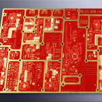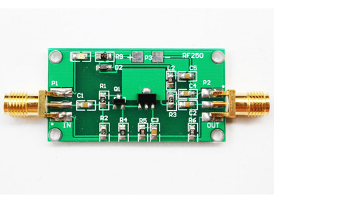
As electronic systems become faster, smaller, and more integrated, PCB designers must consider much more than basic electrical connectivity. High-Frequency PCB designs require careful control of routing geometry, reference planes, return-current paths, power distribution, differential signals, and electromagnetic compatibility.
At the same time, ESD and EMI can significantly affect sensitive digital, analog, display, and communication circuits. A good PCB layout should therefore consider signal integrity, power integrity, grounding, shielding, and protection as part of one integrated design strategy.
The following questions and answers summarize several practical principles for PCB Routing, grounding, testing, and ESD protection.
1. How Should Differential Pairs Be Routed?
Differential signaling is widely used in high-speed interfaces because it can improve noise immunity and reduce susceptibility to common-mode interference when properly implemented.
Modern PCB design tools can define a differential pair as a constrained routing object. Once the pair is configured, the routing system can maintain key parameters such as:
- Trace width.
- Differential spacing.
- Pair-to-pair spacing.
- Relative length.
- Layer assignment.
- Via transitions.
- Routing clearance.
The two traces should generally be routed together and maintain consistent geometry.
When an obstacle is encountered, the pair may need to separate temporarily. However, unnecessary separation should be minimized because large asymmetry can increase skew and common-mode conversion.
For layer transitions, designers should also consider the return-current path. If a differential pair changes layers, appropriate reference-plane continuity and ground-via structures may be required.
Differential Pair Routing Best Practices
For Differential Pair Routing, designers should:
- Keep the two traces close and geometrically consistent.
- Maintain an appropriate differential impedance.
- Minimize unnecessary vias.
- Avoid abrupt width changes.
- Avoid long parallel coupling with unrelated aggressive signals.
- Maintain a suitable reference plane.
- Keep the electrical lengths within the requirements of the interface.
- Match the via structure of the two traces where practical.
Equal physical length alone does not guarantee good differential performance. The complete electrical path must be considered.
2. How Should Power and Ground Planes Be Arranged in a Multilayer PCB?
Suppose a 12-layer PCB contains several power rails, such as 2.2 V, 3.3 V, and 5 V.
It is not necessary to place all power rails on a single layer in every design. The correct layer assignment depends on the stackup, current requirements, noise sensitivity, power distribution, and routing density.
For multilayer boards, designers should consider the relationship between:
- Signal layers.
- Power planes.
- Ground planes.
- Dielectric thickness.
- Return-current paths.
- Power distribution impedance.
A signal routed over a continuous reference plane generally has a more predictable return-current path.
This is particularly important for High-Frequency PCB designs.
Power and Ground Plane Coupling
Power and ground planes can form a low-inductance power-distribution structure when appropriately arranged.
However, simply placing a power plane next to a ground plane does not automatically guarantee good power integrity.
Engineers should evaluate:
- Plane geometry.
- Plane-to-plane spacing.
- Current distribution.
- Decoupling.
- Resonance.
- Layer transitions.
- Load locations.
- High-frequency return paths.
For multiple power rails, the power architecture should also prevent unwanted coupling between noisy and sensitive domains.
3. How Can PCB Manufacturers Verify the Finished PCB?
Before a PCB is released for assembly or shipment, manufacturers typically perform inspections and electrical tests appropriate to the product requirements.
Common methods include:
Automated Optical Inspection
AOI can identify many manufacturing defects, including:
- Open or shorted copper features.
- Incorrect patterns.
- Missing or abnormal pads.
- Solder mask-related defects.
- Registration issues.
Electrical Testing
Electrical testing can verify whether the manufactured board contains unintended opens or shorts.
Depending on production volume and product requirements, manufacturers may use:
- Flying-probe testing.
- Fixture-based electrical testing.
- Continuity testing.
- Isolation testing.
X-Ray Inspection
X-ray inspection can be useful for structures that cannot be fully evaluated from the PCB surface.
It may help inspect:
- Hidden solder joints.
- BGA connections.
- Certain internal structures.
- Plated or filled features where applicable.
X-ray is not a universal replacement for other inspection methods. The appropriate inspection technique depends on the product structure and failure mode being investigated.
PCB Testing After Assembly
For assembled boards, additional testing may include:
- ICT.
- Functional testing.
- AOI.
- X-ray inspection.
- Boundary-scan testing where applicable.
ICT test points should be considered during the PCB design stage if ICT will be used in production.
Therefore, PCB Testing should be considered during design rather than added only after the PCB has been manufactured.
4. What Does Enclosure Shielding Mean?
The original concept of “organizational protection” is better understood as system-level shielding and enclosure protection.
For products that are sensitive to electromagnetic interference, the enclosure can become part of the overall EMC strategy.
A conductive enclosure can help contain or reduce electromagnetic coupling when it is properly designed and electrically integrated.
However, the enclosure alone does not guarantee EMC performance.
Engineers must also consider:
- Openings and seams.
- Cable entry points.
- Connector locations.
- Shield-to-ground connections.
- PCB grounding.
- Internal return-current paths.
- Display interfaces.
- Antenna structures.
- Shielding materials.
For RF products, the enclosure and PCB should be designed together.
5. Should ESD Be Considered When Selecting ICs?
Yes. ESD should be considered at both the component and system levels.
Some ICs include integrated ESD protection structures, but the level of protection varies by device and interface.
When selecting an IC, engineers should review the manufacturer’s specifications for:
- ESD ratings.
- Human Body Model (HBM).
- Charged Device Model (CDM).
- Operating voltage.
- Absolute maximum ratings.
- Recommended protection circuits.
However, the ESD rating of an IC does not mean that the complete product will automatically pass system-level ESD testing.
A product can still fail because an ESD event couples into:
- Signal traces.
- Power rails.
- Ground structures.
- Connectors.
- Buttons.
- Display interfaces.
- Cables.
- Mechanical openings.
Therefore, ESD Protection should be designed at multiple levels.
6. Should a PCB Ground Plane Form a Closed Loop?
Not necessarily.
The original recommendation to always use a “tree-shaped” ground structure is too broad.
A better principle is to minimize unnecessary loop area while maintaining a low-impedance and predictable return-current path.
For high-speed and high-frequency circuits, the return current tends to follow the path of lowest impedance, which is strongly influenced by the reference plane and frequency.
A continuous ground plane can often provide an effective return path.
However, ground-plane design must also consider:
- Analog and digital partitioning.
- High-current switching circuits.
- RF sections.
- Sensitive analog circuits.
- Connector locations.
- Cable interfaces.
- Chassis connections.
- EMI requirements.
Ground Design Principles
For PCB Grounding:
- Use continuous reference planes where practical.
- Minimize unnecessary return-path discontinuities.
- Avoid forcing high-frequency return currents through long detours.
- Keep high-current switching loops compact.
- Place ground vias near critical transitions when appropriate.
- Separate noisy and sensitive circuits through placement and routing.
- Avoid creating unintended antenna-like structures.
The goal is controlled current flow rather than simply creating as much copper as possible.
7. Should Different Power Supplies Share the Same Ground?
There is no universal answer.
If two power supplies belong to the same electrical system, they may need a common reference depending on how the signals and interfaces between them are defined.
For example, if two circuits exchange single-ended signals, they generally require a defined common reference or another suitable return path.
If two power domains need electrical isolation, their grounds may intentionally remain isolated and signals may be transferred through:
- Digital isolators.
- Optocouplers.
- Transformers.
- Isolated transceivers.
- Other isolation structures.
Therefore, the decision should be based on the system architecture rather than a simple rule that all grounds must be connected or must remain separate.
Grounding Should Follow the Signal Path
When multiple power domains exist, ask:
Where does the signal current return?
This question is often more useful than simply asking whether two ground planes should be connected.
Good Power Integrity and signal-integrity design require a predictable current-return structure.
8. Should Multiple PCBs in One System Share a Common Ground?
Again, the answer depends on the system architecture.
If multiple PCBs form one electrically connected system, they often require a common reference or a deliberately defined grounding structure.
However, the boards may also contain isolated domains.
When multiple PCBs are connected through cables or connectors, designers should carefully consider:
- Ground potential differences.
- Return-current paths.
- Connector pin assignment.
- Cable shielding.
- Chassis connections.
- Common-mode currents.
- ESD paths.
- EMI coupling.
A poorly designed inter-board connection can become an important source of EMI.
For this reason, grounding should be considered at the system level rather than treating each PCB as an independent object.
9. How Can a Metal-Enclosure Handheld Product Improve ESD Performance?
Handheld products with metal enclosures can present additional ESD challenges because the enclosure may become a direct discharge path or couple the transient energy into internal circuits.
Consider a product containing:
- LCD display.
- CPU.
- Metal enclosure.
- Flexible cables.
- External buttons.
- Connectors.
- Battery or power interface.
If an ESD test produces failures at relatively low contact or air-discharge levels, the first step should be to identify the coupling path.
Possible ESD Coupling Paths
ESD can enter through:
- Metal enclosure.
- Buttons.
- Connector shells.
- Display openings.
- Cable shields.
- Touch interfaces.
- Mechanical gaps.
- PCB mounting points.
The design strategy may include:
- Providing a controlled chassis discharge path.
- Separating the ESD current path from sensitive PCB circuitry.
- Adding appropriate TVS or transient protection.
- Improving grounding and return-current paths.
- Strengthening connector protection.
- Improving display-interface protection.
- Reducing coupling into sensitive signal traces.
- Optimizing enclosure seams and openings.
The correct solution depends on the mechanical construction and electrical architecture.
Simply connecting the metal enclosure directly to PCB ground is not always the correct solution. In some systems, chassis ground and circuit ground may need to be connected at a controlled location or through an appropriate EMC structure.
10. How Should a DSP and PLD System Be Designed for ESD Protection?
Systems containing DSPs, PLDs, CPUs, or other high-speed digital devices can be sensitive to ESD because these devices often contain fast internal switching structures and multiple external interfaces.
During system design, identify all points that can be directly touched or connected to external equipment.
Particular attention should be given to:
- USB interfaces.
- Ethernet interfaces.
- Buttons.
- Displays.
- Keypads.
- Communication ports.
- Power connectors.
- External cables.
- Metal enclosure interfaces.
Multi-Level ESD Protection
A robust ESD Protection strategy can include:
Level 1: Mechanical Protection
Reduce direct ESD coupling through enclosure and interface design.
Level 2: Interface Protection
Place suitable protection components close to external connectors and entry points.
Level 3: PCB-Level Protection
Control routing, grounding, return paths, and sensitive circuit placement.
Level 4: Component-Level Protection
Use ICs and interface components with appropriate ESD performance.
Level 5: System-Level Validation
Perform ESD testing under the applicable standard and verify both hardware and software behavior.
11. Why Can ESD Cause an LCD or CPU to Malfunction?
An ESD event does not necessarily destroy a component.
It can also cause temporary or intermittent malfunction.
Possible effects include:
- CPU reset.
- System lockup.
- Display flicker.
- LCD artifacts.
- Communication errors.
- Data corruption.
- Touchscreen malfunction.
- Unexpected restart.
- Permanent component damage.
The ESD transient may couple into the system through power or signal paths.
For example, an ESD event near a display interface can produce a transient that couples into high-speed display signals or the associated power distribution network.
This is why EMI Control and ESD design should not be considered completely separate from PCB layout.
12. Does CPU Frequency Determine ESD Performance?
Not directly.
A CPU operating at 33 MHz can still be highly sensitive to ESD.
The fundamental frequency of a digital clock is only one part of the electromagnetic behavior. Fast signal edges contain significant higher-frequency spectral components.
Therefore, ESD and EMI performance depends on many factors, including:
- Signal rise and fall time.
- PCB stackup.
- Return-current paths.
- Ground impedance.
- Power distribution.
- Cable routing.
- Enclosure construction.
- Protection devices.
- Connector design.
- Mechanical structure.
- Software recovery behavior.
A lower clock frequency does not automatically mean that a product will be immune to ESD problems.
13. How to Diagnose an ESD Test Failure
When a product fails an ESD test, changing components randomly is usually inefficient.
A structured troubleshooting process is more effective.
Step 1: Identify the Failure Threshold
Record the discharge type and level at which the failure occurs.
Step 2: Identify the Failure Location
Determine whether the failure originates near:
- Connector.
- Display.
- Button.
- Enclosure.
- Cable.
- PCB edge.
- Power input.
Step 3: Identify the Failure Symptom
Determine whether the product experiences:
- Reset.
- Freeze.
- Display corruption.
- Communication failure.
- Permanent damage.
Step 4: Trace the Coupling Path
Determine how the ESD transient reaches the sensitive circuit.
Step 5: Improve the Current Path
Create a controlled path for the ESD current that minimizes coupling into sensitive circuitry.
Step 6: Add or Optimize Protection
Protection components should be positioned according to the actual current path and interface structure.
Step 7: Retest the Product
Repeat the ESD test under controlled conditions and compare the results.
14. The Relationship Between PCB Routing, EMI and ESD
PCB Routing, PCB Grounding, EMI Control, and ESD Protection are closely related.
A poorly designed PCB may provide multiple unintended paths for transient and high-frequency currents.
For example:
ESD Source → Enclosure/Connector → PCB Entry Point → Ground/Power Structure → Sensitive Circuit
The objective is to control this path.
A good design should prevent the transient from passing through sensitive signal or power circuitry whenever possible.
This requires coordination between:
- PCB layout.
- Mechanical design.
- Grounding.
- Shielding.
- Protection components.
- Cable design.
- Connector design.
15. PCB Design Checklist for High-Frequency and ESD Applications
Before finalizing a high-speed PCB, engineers should review the following items:
Signal Routing
- Are critical signals routed with controlled geometry?
- Are differential pairs properly constrained?
- Are unnecessary vias minimized?
- Are high-speed traces kept away from noisy circuits?
Grounding
- Is the reference plane continuous?
- Are return-current paths clearly defined?
- Are high-current loops minimized?
- Are ground transitions properly connected?
Power Integrity
- Are power and ground structures appropriately arranged?
- Are decoupling capacitors positioned close to their loads?
- Are noisy power domains separated from sensitive circuits where necessary?
ESD Protection
- Are external interfaces protected?
- Is the ESD current path controlled?
- Is the enclosure integrated into the EMC strategy?
- Are sensitive ICs adequately protected?
PCB Testing
- Are electrical test requirements defined?
- Are ICT test points included where needed?
- Is AOI coverage adequate?
- Is X-ray inspection required for hidden structures?
- Has system-level ESD testing been planned?
16. Kingda’s Approach to Reliable PCB Manufacturing
A reliable PCB design must eventually be converted into a physical product with controlled manufacturing tolerances.
Kingda can support customers by coordinating PCB design requirements with manufacturing considerations such as:
- Layer stackup.
- Material selection.
- Controlled impedance.
- Copper thickness.
- Via structures.
- Registration accuracy.
- Surface finish.
- Electrical testing.
- DFM review.
For high-speed and high-reliability products, manufacturing variation can influence the final electrical performance. Therefore, design constraints should be established together with realistic production capabilities.
Conclusion
High-frequency PCB design is not simply a matter of routing traces at high speed. Reliable performance depends on the interaction between PCB Routing, differential signaling, reference planes, grounding, power distribution, shielding, and manufacturing quality.
For ESD-sensitive products, the mechanical enclosure, connectors, cables, PCB layout, protection devices, and grounding structure should be treated as one complete system.
The most effective strategy is to control current paths—both normal signal return currents and abnormal transient currents—rather than relying on isolated rules such as “all grounds must be connected” or “all grounds must be separated.”
By combining disciplined Differential Pair Routing, controlled PCB Grounding, strong Power Integrity, appropriate ESD Protection, and systematic PCB Testing, engineers can significantly improve the robustness and reliability of high-speed electronic products.