The global PCB Manufacturing industry is highly competitive. As electronic products become smaller, more complex, and more demanding, PCB manufacturers must continuously improve production efficiency, quality, and process consistency.
Customers expect high-quality circuit boards with short lead times and competitive pricing. Meeting these expectations requires more than simply reducing production costs. Manufacturers need to optimize every stage of the PCB Manufacturing Process, from design preparation and material selection to fabrication, inspection, panel separation, and final testing.
Using appropriate software, modern production equipment, reliable process controls, and advanced manufacturing technologies can help manufacturers reduce unnecessary processing, improve yield, and deliver more consistent products.
For companies such as Kingda, continuous PCB Process Optimization is an important part of supporting customers with reliable and cost-effective PCB solutions.
Here are five practical approaches that can help improve modern PCB production.
1. Use Professional PCB Design Software
Modern PCBs are becoming increasingly compact and sophisticated.
Consumer electronics, communication equipment, automotive systems, industrial controls, and other electronic products require more functions within smaller physical spaces. This creates increasingly demanding requirements for component placement, routing, signal integrity, manufacturability, and board reliability.
Professional PCB Design Software can help engineers manage these requirements more efficiently.
Modern design platforms typically provide functions such as:
- Schematic capture
- PCB layout
- Design Rule Check (DRC)
- Component libraries
- Stackup configuration
- Controlled-impedance planning
- Differential-pair routing
- Manufacturing rule verification
- Gerber and manufacturing-data generation
- Design templates
Design-rule checking is particularly useful because it can identify potential problems before the design reaches fabrication.
Typical checks may include:
- Minimum trace width
- Minimum spacing
- Pad dimensions
- Via sizes
- Copper-to-edge clearance
- Solder mask clearance
- Hole-to-hole spacing
- Manufacturing constraints
Designers can also create reusable templates for commonly produced board structures.
This can shorten engineering preparation time and improve consistency between different projects.
Design for Manufacturing
Software alone, however, cannot replace communication with the PCB manufacturer.
A strong DFM approach should consider the manufacturer’s actual process capabilities, including minimum line width and spacing, drilling capability, layer registration, material availability, surface finish, and production tolerances.
When DFM requirements are considered during the design stage, potential manufacturing problems can be identified before production begins.
This can reduce engineering changes, production delays, scrap, and unnecessary development costs.
2. Apply High-Quality Solder Mask
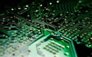
Solder Mask is an important part of modern PCB fabrication.
It is a protective coating applied over selected areas of the PCB surface. It helps protect copper from environmental exposure and reduces the risk of accidental solder bridging during assembly.
As PCB designs become denser, solder mask registration and process control become increasingly important.
A properly controlled solder mask process can help provide:
- Protection for exposed copper
- Electrical insulation between conductive features
- Reduced solder bridging
- Better surface durability
- Clear definition of solderable pads
- Improved assembly consistency
Poor solder mask quality can create problems such as insufficient clearance, pad coverage, solder bridges, and visual defects.
Therefore, solder mask should be treated as an important manufacturing process rather than simply a cosmetic coating.
Solder Mask and Fine-Pitch PCB Design
Fine-pitch components require precise alignment between solder mask openings and copper pads.
As component pitch decreases, manufacturing tolerances become more critical.
PCB manufacturers should therefore control:
- Solder mask thickness
- Registration accuracy
- Opening dimensions
- Exposure parameters
- Developing conditions
- Curing conditions
- Surface cleanliness
These controls become particularly important for HDI boards, fine-pitch BGA applications, and high-density electronic assemblies.
3. Optimize PCB Etching and Chemical Processes
Etching is one of the fundamental processes in PCB Production.
During fabrication, unwanted copper is removed to form the required circuit pattern.
However, etching quality directly influences the final trace geometry.
Poor process control can result in:
- Excessive undercut
- Over-etching
- Incomplete etching
- Trace-width variation
- Uneven copper removal
- Reduced manufacturing yield
For this reason, modern PCB manufacturers focus on controlling the complete etching process rather than simply selecting an etching chemical.
Important parameters may include:
- Etching chemistry
- Chemical concentration
- Temperature
- Spray pressure
- Conveyor speed
- Copper thickness
- Panel loading
- Chemical replenishment
Why Process Control Matters
As line widths and spacing become smaller, even minor variations in etching can affect electrical performance and manufacturability.
Fine-line PCB production therefore requires stable process conditions and continuous monitoring.
Automated chemical management and process-control systems can help maintain consistent etching performance and reduce variation between production batches.
Environmental and Safety Considerations
Modern PCB Manufacturing should also consider environmental protection and chemical safety.
Chemical processes require appropriate:
- Wastewater treatment
- Chemical storage
- Exhaust management
- Employee protection
- Waste disposal
- Regulatory compliance
Manufacturers should follow applicable environmental and occupational-safety requirements rather than relying on improvised chemical handling methods.
Process optimization should improve efficiency while maintaining environmental and workplace safety.
4. Use UV Laser Technology for PCB Panel Separation
As electronic products become smaller and PCB structures become more delicate, panel separation has become an increasingly important manufacturing consideration.
Traditional mechanical separation methods may include:
- Routing
- Punching
- Sawing
- V-cut separation
These methods can be effective for many PCB products, but mechanical cutting can introduce physical stress, vibration, or localized mechanical forces.
For thin, flexible, or mechanically sensitive boards, non-contact processing technologies can provide additional advantages.
UV Laser PCB Cutting is one technology that can be considered for precision panel separation and other fine-feature applications.
Advantages of UV Laser Processing
UV laser processing uses a non-contact beam to remove or cut material.
Potential benefits include:
- Reduced mechanical stress
- High processing precision
- Small cutting features
- Reduced tool wear
- Flexible processing of complex shapes
- Suitable for thin and delicate PCB structures
Because the process does not require a physical cutting tool to contact the board, mechanical deformation can be reduced.
This can be useful for applications involving thin PCBs, compact electronics, flexible circuits, and complex board outlines.
UV Laser vs. Mechanical Separation
The appropriate panel-separation technology depends on the PCB material, thickness, board outline, production volume, dimensional tolerance, and cost target.
Mechanical routing may remain an efficient solution for many conventional rigid PCBs.
UV laser processing becomes more attractive when higher precision, smaller features, or reduced mechanical stress are important.
Therefore, manufacturers should select the separation method according to the actual production requirements rather than assuming that one technology is suitable for every PCB
5. Improve Overall PCB Manufacturing Efficiency
The most important principle of PCB Process Optimization is that manufacturing efficiency should be considered as a complete system.
Improving one individual process does not necessarily improve the entire production line.
For example, faster fabrication is not beneficial if it results in:
- Higher defect rates
- More rework
- Increased scrap
- Lower reliability
- Additional inspection time
- Customer complaints
A truly efficient PCB Manufacturing Process should balance:
Quality + Cost + Lead Time + Yield + Reliability + Safety
Manufacturers should therefore evaluate the complete production flow.
Key Areas for Improvement
Engineering Preparation
Improve manufacturing-data preparation and DFM review before production.
Material Management
Use appropriate materials and establish effective inventory and storage controls.
Production Equipment
Maintain production equipment regularly and replace outdated equipment when it limits process capability.
Process Control
Monitor critical parameters continuously and establish clear process windows.
Automated Inspection
Use AOI, electrical testing, and other inspection technologies to identify defects efficiently.
Yield Management
Analyze recurring defects and determine their root causes instead of repeatedly correcting individual boards.
Production Data
Use manufacturing data to identify process variation and opportunities for improvement.
6. Why Automation Matters in Modern PCB Production
Automation is becoming increasingly important as PCB structures become more complex.
Automated systems can improve consistency in areas such as:
- Material handling
- Drilling
- Imaging
- Etching
- Plating
- Optical inspection
- Electrical testing
- Panel separation
- Production tracking
Automation can also reduce dependence on manual operations for repetitive tasks.
However, automation should not be implemented simply because a process is automated.
The investment should be evaluated according to:
- Production volume
- Required precision
- Labor requirements
- Defect rates
- Equipment utilization
- Maintenance costs
- Expected return on investment
The goal is to create a stable and efficient manufacturing system rather than simply adding more equipment.
7. Improve PCB Yield Through Root-Cause Analysis
Yield is one of the most important indicators of PCB Manufacturing Efficiency.
A production line with high output but low yield may ultimately be less efficient than a slower line with stable quality.
Manufacturers should track defects and identify recurring patterns.
Common PCB manufacturing defects may include:
- Open circuits
- Short circuits
- Insufficient plating
- Over-etching
- Drilling defects
- Registration errors
- Solder mask defects
- Surface-finish problems
- Contamination
- Lamination defects
Root-cause analysis can help determine whether a defect originates from:
Material → Equipment → Process → Operator → Environment → Design
Corrective actions should focus on eliminating the source of the problem rather than repeatedly repairing defective boards.
8. Improve Communication Between PCB Design and Manufacturing
Efficient production begins before the PCB reaches the factory.
Design engineers and manufacturing engineers should communicate early about:
- Board materials
- Layer count
- Stackup
- Trace width and spacing
- Via structures
- Impedance requirements
- Surface finish
- Solder mask
- Panelization
- Dimensional tolerances
- Testing requirements
A design that is electrically functional may still be unnecessarily difficult or expensive to manufacture.
For example, using extremely small features when they provide little functional benefit can increase fabrication complexity without improving the final product.
A practical DFM review can help designers balance electrical requirements with manufacturing capability.
9. Kingda’s Approach to Efficient PCB Manufacturing
Kingda recognizes that manufacturing efficiency is closely connected to process control, engineering preparation, equipment capability, and quality management.
For different PCB projects, the appropriate manufacturing process should be selected according to the board’s technical requirements rather than applying the same production method to every design.
Kingda’s engineering review can evaluate areas such as:
- PCB stackup
- Material selection
- Line width and spacing
- Drilling requirements
- Via structures
- Solder mask
- Surface finish
- Panelization
- Manufacturing tolerances
- Electrical testing
- DFM considerations
Early technical communication can help identify potential production challenges before fabrication begins.
This approach can reduce unnecessary design revisions and help customers achieve more predictable manufacturing results.

10. The Future of PCB Manufacturing Technology
The PCB Production industry will continue to evolve as electronic products become smaller, faster, and more integrated.
Future manufacturing development is likely to focus on:
- Higher automation
- More precise imaging
- Advanced laser processing
- Finer circuit geometries
- Improved registration accuracy
- Smarter production monitoring
- Automated inspection
- Better process traceability
- More efficient resource utilization
- Environmentally responsible manufacturing
Manufacturers that continuously improve their processes will be better positioned to meet increasingly demanding customer requirements.
However, technological advancement should always be connected to practical manufacturing value.
The most advanced equipment is not necessarily the best solution for every production line.
The right combination of equipment, process capability, engineering expertise, quality control, and production management is what creates a truly efficient manufacturing system.
Conclusion
A competitive PCB Manufacturing operation requires continuous improvement rather than simply reducing production costs.
Professional PCB Design Software, reliable Solder Mask processes, controlled etching, advanced UV Laser PCB Cutting, automation, DFM review, and systematic quality management can all contribute to better manufacturing efficiency.
At the same time, manufacturers must maintain a balance between quality, cost, production speed, reliability, environmental responsibility, and safety.
As PCB structures become increasingly dense and complex, manufacturing capability will become even more important.
By continuously optimizing its PCB Manufacturing Process, adopting appropriate technologies, and working closely with customers during the engineering stage, Kingda can support the development of reliable, manufacturable, and cost-effective PCB products.