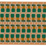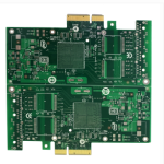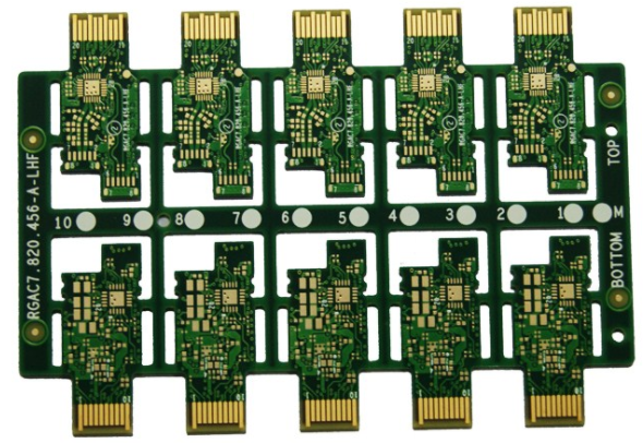
As electronic products become smaller, faster, and more highly integrated, conventional PCB structures are increasingly challenged by limited routing space and component density. This has driven the development of HDI PCB technology.
HDI stands for High-Density Interconnect. An HDI Circuit Board uses technologies such as microvias, blind vias, buried vias, and sequential lamination to achieve a higher wiring density within a smaller PCB area.
Compared with a conventional PCB, an HDI board can provide more routing channels, finer interconnections, smaller via structures, and greater flexibility in component placement.
However, simply having blind or buried vias does not automatically mean that a board is an HDI PCB. The actual structure and manufacturing technology must be considered.
What Is an HDI PCB?
An HDI PCB is a printed circuit board manufactured using high-density interconnection technologies.
Compared with a conventional multilayer PCB, an HDI board typically uses smaller microvias and more advanced layer-building methods to increase interconnection density.
The main technologies associated with HDI include:
- Microvias
- Blind vias
- Buried vias
- Fine-line routing
- Fine-pitch interconnections
- Sequential lamination
- High-precision registration
Microvias are generally very small vias, commonly formed using laser drilling. They are particularly useful for connecting high-density component areas such as BGA packages.
The primary purpose of these technologies is to create more routing space while reducing the overall size of the PCB.
What Is a Conventional PCB?
A Conventional PCB generally refers to a traditional PCB structure manufactured using established processes such as mechanical drilling, through-hole plating, copper patterning, and conventional lamination.
Traditional PCBs can be:
- Single-sided
- Double-sided
- Multilayer
They remain widely used because they offer a good balance between performance, manufacturing complexity, and cost.
FR-4 is one of the most commonly used substrate families for conventional PCBs, although different applications may require specialized materials.
Conventional PCB technology is suitable for many electronic products where component density and routing requirements are not extremely demanding.
HDI PCB vs. Conventional PCB
The main difference between an HDI PCB and a conventional PCB is not simply the number of layers.
The key difference is the interconnection technology used to create a higher wiring density.
| Feature | Conventional PCB | HDI PCB |
|---|---|---|
| Interconnection | Mainly through vias | Microvias, blind vias, buried vias, and through vias |
| Drilling | Mainly mechanical drilling | Mechanical and laser drilling |
| Line/space | Conventional | Typically finer |
| Component density | Moderate | High |
| BGA routing | More challenging at very fine pitch | Better suited to fine-pitch BGA |
| Layer structure | Conventional lamination | May use sequential lamination |
| Manufacturing complexity | Relatively lower | Higher |
| Cost | Generally lower | Generally higher |
| Typical applications | General electronics | Smartphones, wearables, advanced computing, automotive, communications |
The appropriate structure depends on the product’s electrical, mechanical, thermal, and manufacturing requirements.
Are PCBs With Blind and Buried Vias Automatically HDI?
No.
A PCB containing Blind Via or Buried Via is not necessarily an HDI PCB.
Blind and buried vias are structural technologies that can also be used in conventional multilayer PCB designs.
An HDI classification generally involves a combination of high-density design characteristics, microvia technology, fine-line routing, and sequential build-up processes.
Therefore, the PCB structure should be evaluated as a whole rather than classified solely according to whether blind or buried vias are present.
What Is a Microvia?
A Microvia is a small-diameter via commonly produced using laser drilling.
Microvias are particularly useful when routing high-density component packages such as BGAs.
Because the via occupies less PCB area than a conventional mechanically drilled through-hole, it allows designers to place routing traces closer together and create more efficient interconnections.
Microvias may connect:
- Outer layer to the adjacent inner layer
- One build-up layer to another
- Multiple layers through appropriate stacked or staggered structures
The exact microvia dimensions depend on the PCB manufacturer’s process capability, material system, layer thickness, and design requirements.
What Is a Blind Via?
A Blind Via connects an outer PCB layer to one or more internal layers without passing completely through the entire board.
For example, a blind via may connect Layer 1 to Layer 2 or Layer 3 while remaining isolated from the deeper layers.
In HDI structures, laser-drilled microvias are commonly used as blind vias.
This allows designers to create short interconnection paths while freeing up routing space on other layers.
For a four-layer board, for example, a build-up structure may include connections between Layers 1–2 and Layers 3–4.
For a six-layer board, possible build-up structures may include Layers 1–2 and Layers 5–6.
However, the actual structure depends on the specific stack-up and design requirements.
What Is a Buried Via?
A Buried Via connects internal layers without reaching either external surface of the PCB.
For example, a buried via may connect Layer 2 to Layer 5 inside a multilayer PCB.
Because the via is completely contained within the board, it cannot be accessed directly from the external surface.
Buried vias can provide additional routing flexibility, but they also increase manufacturing complexity because the relevant inner-layer structure generally needs to be fabricated before the complete board is laminated.
What Is a Sequential Build-Up Process?
One of the defining technologies associated with HDI is sequential lamination.
Unlike a conventional multilayer PCB that may be laminated as a complete stack and then mechanically drilled, an HDI board can be constructed through multiple lamination stages.
A simplified build-up sequence can be understood as:
Core → lamination → laser drilling → copper processing → additional build-up → laser drilling → final lamination
The exact process varies depending on the HDI structure.
Sequential build-up provides designers with greater freedom to place microvias and routing layers where they are needed.
What Is First-Order HDI?
First-order HDI is one of the simpler HDI structures.
A typical first-order structure uses microvias or blind vias connecting an outer layer to its adjacent inner layer.
For example:
Layer 1 → Layer 2
and/or
Layer n → Layer n-1
The outer build-up layers are added to the core structure, followed by laser drilling and subsequent copper processing.
First-order HDI is generally easier to manufacture than more complex HDI structures because the number of sequential build-up operations is limited.
What Is Second-Order HDI?
Second-order HDI involves a more complex build-up structure and additional sequential processing.
Depending on the design, second-order structures can use stacked or staggered microvias.
A simplified example is:
Layer 1 → Layer 2 → Layer 3
or a structure in which two HDI build-up stages are incorporated around a central core.
Compared with first-order HDI, second-order structures require tighter control of:
- Layer registration
- Laser drilling
- Copper plating
- Via alignment
- Lamination
- Via reliability
This makes manufacturing process control increasingly important.
What Is Third-Order HDI?
Third-order HDI involves an additional build-up sequence and is more complex than first- and second-order structures.
A simplified multilayer structure may contain multiple sequential build-up layers around a central core.
As the HDI order increases, the manufacturing process generally becomes more demanding because more sequential lamination, drilling, plating, and registration operations are required.
The actual classification should always be based on the specific stack-up and manufacturing structure rather than simply counting the number of PCB layers.
Stacked and Staggered Microvias
Microvia structures can generally be arranged in different ways.
Staggered Microvias
In a staggered structure, microvias on adjacent layers are offset from one another.
This structure can simplify certain manufacturing requirements and may provide good reliability depending on the design.
Stacked Microvias
In a stacked structure, microvias are positioned directly above one another across multiple layers.
Stacked microvias can provide very high routing density and are particularly useful in fine-pitch BGA applications.
However, they require more precise manufacturing control, particularly for copper filling, alignment, plating, and reliability.
Why Is HDI Technology Used?
The main purpose of HDI Technology is to increase interconnection density while reducing PCB size or enabling more functionality within the same board area.
Key benefits include:
Higher Wiring Density
Microvias occupy less space than conventional through-holes, creating additional routing channels.
Smaller PCB Size
A high-density design can potentially reduce the required board area.
Better BGA Routing
Fine-pitch BGA packages often require high-density fan-out and escape routing. HDI technology provides more flexible routing options.
More Efficient Layer Utilization
Build-up layers can be added where additional routing capacity is required rather than increasing the entire board’s layer count.
Improved Design Flexibility
Designers have greater freedom to distribute signals, power, and ground connections across the board.
HDI and High-Frequency PCBs Are Not the Same
It is important not to confuse HDI PCB technology with high-frequency PCB technology.
HDI describes an interconnection and manufacturing approach focused primarily on increasing wiring density.
High-frequency PCB technology focuses on electrical performance at high frequencies, including:
- Dielectric constant
- Dissipation factor
- Insertion loss
- Signal loss
- Impedance control
- Material stability
An HDI PCB can also be designed for high-frequency applications, but HDI itself does not automatically mean that the PCB is a high-frequency board.
The two technologies address different aspects of PCB performance and can be combined when required.
Materials Used for HDI PCBs
Material selection is particularly important in high-density PCB manufacturing.
Depending on the application, HDI boards may use:
- FR-4
- High-Tg FR-4
- Low-loss laminates
- High-frequency materials
- Thin core materials
- Specialized build-up dielectric materials
Traditional HDI structures often use build-up dielectric materials with suitable resin systems for laser drilling.
The material must provide appropriate mechanical, thermal, and electrical properties while also supporting reliable microvia formation.
Manufacturing Challenges of HDI PCBs
Compared with conventional PCB manufacturing, PCB Manufacturing for HDI structures requires tighter process control.
Important manufacturing challenges include:
Registration Accuracy
Each sequential lamination and drilling step must maintain accurate alignment between layers.
Small registration errors can cause microvias to miss their target pads.
Laser Drilling Quality
Laser drilling must produce consistent microvia dimensions and reliable connections.
Factors such as material composition, dielectric thickness, laser parameters, and copper characteristics can influence drilling quality.
Copper Plating
Reliable microvia connections require controlled copper deposition and appropriate plating quality.
This becomes increasingly important for stacked microvias.
Lamination Control
Sequential lamination requires accurate control of temperature, pressure, resin flow, and layer alignment.
Via Reliability
Microvias experience thermal and mechanical stresses during assembly and product operation. Proper material selection and process control are therefore essential.
How to Determine Whether a PCB Is HDI
When reviewing a PCB design, do not classify it as HDI simply because it contains blind or buried vias.
A more reliable evaluation should consider:
- Whether microvias are used
- Whether laser drilling is required
- Whether sequential lamination is used
- Whether build-up dielectric layers are present
- Whether fine-line and fine-pitch routing is required
- Whether blind or buried microvias are incorporated
- Whether the board uses high-density interconnection structures
The final classification should be confirmed by the PCB manufacturer based on the actual stack-up and manufacturing process.
When Should You Choose HDI PCB?
An HDI Circuit Board is particularly suitable when the product requires high component density but has limited PCB space.
Typical applications include:
- Smartphones
- Wearable electronics
- Tablets
- Advanced computing equipment
- Automotive electronics
- Communication systems
- Medical electronics
- High-density industrial equipment
- Compact consumer electronics
For simple electronic products with sufficient board space and relatively low routing density, a conventional PCB may provide a more economical solution.
Kingda’s HDI PCB Manufacturing Capabilities
Kingda provides PCB manufacturing solutions for demanding high-density applications, including multilayer PCBs, HDI PCB structures, blind and buried vias, fine-line designs, high-frequency PCBs, thick-copper boards, prototypes, and volume production.
HDI manufacturing requires close coordination between PCB design and fabrication. During the engineering review process, factors such as stack-up structure, microvia dimensions, material selection, layer registration, copper thickness, and manufacturing tolerances should be evaluated before production.
This design-for-manufacturing approach helps reduce fabrication risks and improve the consistency and reliability of high-density PCBs.
Conclusion
The main difference between an HDI PCB and a conventional PCB is the way high-density interconnections are achieved.
HDI technology uses Microvia, Blind Via, Buried Via, fine-line routing, and sequential build-up processes to provide greater routing density within a limited PCB area.
First-order, second-order, and third-order HDI structures represent different levels of build-up complexity. As the HDI order increases, requirements for registration accuracy, laser drilling, copper plating, lamination, and process control also become more demanding.
It is also important to remember that a PCB with blind or buried vias is not automatically an HDI board. The complete interconnection structure and manufacturing process must be evaluated.
As electronic products continue to become smaller and more highly integrated, HDI Technology will remain an important solution for achieving higher PCB density, better component integration, and more compact electronic designs.