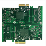
Although some high-power RF PCB applications operate independently of base stations, many of the highest-power PCB applications are associated with the power amplifiers used in wireless communication infrastructure. Designing these circuits requires careful consideration of electrical performance, thermal behavior, material properties, and long-term reliability.
This article focuses on the fundamental considerations involved in designing High-Power RF PCB applications, particularly those used in base-station power amplifiers. However, the same principles can also be applied to other high-power and high-frequency electronic systems.
Why Thermal Management Matters in High-Power RF PCB Design
Thermal management is one of the most important considerations in high-power RF applications. When RF power is transmitted through a circuit, part of that energy is converted into heat because of electrical and material losses.
In general, higher circuit loss results in greater heat generation. Frequency also plays an important role. As operating frequency increases, conductor and dielectric losses can become more significant, potentially increasing the temperature of the circuit.
The relationship between temperature and dielectric properties is another important consideration. As the temperature of a dielectric material changes, its dielectric constant, or Dk, can also change. This temperature dependence is commonly described by the temperature coefficient of dielectric constant (TCDk).
A change in Dk can alter the electrical characteristics of an RF transmission line. In precision RF circuits, this can affect impedance, phase characteristics, matching networks, and overall system performance.
For this reason, thermal management should not be treated as a separate mechanical issue. It is closely connected to the electrical performance and reliability of the entire High-Power RF PCB.
Understanding PCB Loss in High-Frequency Applications
When selecting High-Frequency PCB Materials, designers sometimes focus primarily on the material’s dissipation factor, or Df. Df is an important parameter because it represents dielectric loss within the material, but it does not account for all losses occurring in an RF circuit.
The total loss of an RF transmission line is commonly reflected by insertion loss. Several mechanisms contribute to total insertion loss, including:
- Dielectric loss
- Conductor loss
- Radiation loss
- Leakage loss
Therefore, selecting a material with an extremely low Df does not automatically guarantee the lowest possible insertion loss.
The complete transmission-line structure must be evaluated, including the dielectric material, copper foil, conductor geometry, surface roughness, operating frequency, and PCB construction.
Df and Dielectric Loss
Df, also known as the dissipation factor or loss tangent, indicates how much RF energy is dissipated as heat within a dielectric material.
A material with a low Df generally produces lower dielectric loss, making it attractive for high-frequency and high-power applications.
For example, a circuit manufactured using a material with a Df of approximately 0.002 and smooth copper foil can achieve relatively low insertion loss. However, simply selecting a low-loss dielectric material is not enough.
If the same circuit uses rougher electrolytic copper instead of smooth copper foil, conductor loss can increase significantly, particularly at high frequencies.
This demonstrates why material selection for a High-Power RF PCB must consider both dielectric and conductor losses.
Copper Roughness and Insertion Loss
Copper surface roughness has a direct influence on conductor loss in high-frequency circuits.
The copper roughness that matters most is the roughness at the copper-dielectric interface of the laminate. When an RF signal travels along a conductor, current distribution becomes increasingly concentrated near the conductor surface as frequency rises.
This phenomenon is associated with the skin effect. At higher frequencies, the effective current-carrying region becomes smaller, making the electrical impact of copper surface roughness more significant.
Rough copper surfaces effectively increase the path traveled by high-frequency current, which can increase conductor loss and consequently increase Insertion Loss.
The influence of copper roughness becomes even more important when thinner dielectric layers are used. In a thin dielectric structure, the electromagnetic fields interact more closely with the copper-dielectric interface, so the electrical impact of copper roughness can become more pronounced.
Therefore, when designing a high-frequency transmission line, designers should consider copper profile as carefully as they consider the Df of the dielectric material.
Low-Loss Materials for High-Power RF PCB Applications
For many high-power RF applications, selecting laminate materials with low dielectric loss and relatively smooth copper foil can help reduce overall transmission loss.
However, electrical loss is only one part of the material-selection process.
An effective High-Frequency PCB Materials selection should also consider:
- Low Df
- Stable Dk
- Low TCDk
- Smooth copper foil
- High thermal conductivity
- Low moisture absorption
- Stable dimensional characteristics
- Appropriate thermal expansion behavior
- Compatibility with PCB manufacturing processes
- Long-term reliability under high RF power
Among these factors, thermal conductivity can be particularly important for high-power applications.
Thermal Conductivity and Heat Dissipation
A PCB operating at high RF power can generate considerable heat. If this heat cannot be efficiently transferred away from the circuit, excessive temperature rise may cause performance degradation or reliability problems.
A laminate with higher thermal conductivity can help transfer heat away from the circuit and toward a heat spreader, thermal plane, heatsink, or other thermal-management structure.
Effective Thermal Management may involve a combination of:
- High-thermal-conductivity PCB materials
- Thick copper structures
- Large copper planes
- Thermal vias
- Metal heat spreaders
- Heat sinks
- Proper mechanical thermal interfaces
- Optimized component placement
The appropriate approach depends on the RF power level, board structure, operating frequency, enclosure design, and cooling system.
Frequency and Heat Generation
The relationship between frequency and heat generation is another important factor in high-power RF circuit design.
For the same RF power level, a circuit operating at a higher frequency may experience greater losses and therefore a greater temperature rise.
For example, thermal testing of microstrip transmission lines has demonstrated that an 80 W RF load can produce a significantly different temperature rise at different frequencies. In one example, a microstrip circuit operating at approximately 3.6 GHz showed a temperature rise of around 50°C, while the same circuit tested at approximately 6.1 GHz exhibited a temperature rise of around 80°C.
These values should be regarded as application-specific experimental results rather than universal design rules. Actual temperature rise depends on PCB materials, copper geometry, conductor roughness, dielectric thickness, thermal conductivity, ambient conditions, cooling configuration, and measurement methods.
Nevertheless, the example clearly illustrates that increasing frequency can substantially increase thermal stress in high-power RF circuits.
Why Higher Frequency Can Increase PCB Temperature
Several physical mechanisms contribute to increased heat generation at higher frequencies.
Dielectric Loss
The Df of many dielectric materials varies with frequency. As frequency increases, dielectric loss may also increase, converting more RF energy into heat.
Greater dielectric loss contributes to higher Insertion Loss and increased circuit temperature.
Conductor Loss
Conductor loss also generally increases with frequency.
One important reason is the skin effect. As frequency increases, the skin depth decreases, concentrating RF current closer to the conductor surface.
When the copper surface is relatively rough, this effect can become even more significant.
Power Density
Higher-frequency RF circuits can also involve greater electromagnetic field concentration and power density in specific areas of the circuit.
When high RF power is concentrated in a small PCB region, localized heating can become a significant design concern.
Therefore, thermal analysis should consider not only the total input power but also the actual power distribution across the PCB.
The Importance of Dk Stability and TCDk
The temperature coefficient of dielectric constant, or TCDk, is an important but sometimes overlooked material characteristic.
TCDk describes how the dielectric constant changes with temperature. In RF circuits, changes in Dk can alter the effective electrical length of transmission lines and affect impedance and phase characteristics.
This becomes especially important in power amplifier matching networks.
For example, a quarter-wavelength transmission line may be used as part of an impedance-matching network. Its electrical length depends on the dielectric environment.
If Dk changes significantly as the circuit temperature rises, the effective quarter-wavelength condition can shift. As a result, the matching network may move away from its intended operating condition.
This can reduce matching efficiency and potentially affect power amplifier output power, gain, efficiency, and overall stability.
Consequently, low TCDk can be an important consideration when selecting High-Frequency PCB Materials for precision high-power RF applications.
Key Material Selection Criteria
When selecting materials for a High-Power RF PCB, designers should evaluate the entire set of electrical and thermal requirements rather than relying on a single material parameter.
A suitable high-frequency laminate may need to provide:
| Material Property | Importance in High-Power RF PCB |
|---|---|
| Low Df | Reduces dielectric loss and heat generation |
| Stable Dk | Helps maintain predictable impedance and phase characteristics |
| Low TCDk | Reduces electrical drift caused by temperature changes |
| Smooth copper | Helps reduce conductor loss at high frequencies |
| High thermal conductivity | Improves heat transfer away from the circuit |
| Low moisture absorption | Helps maintain stable RF performance |
| Low and stable CTE | Supports dimensional and reliability control |
| Appropriate copper thickness | Supports current capacity and thermal performance |
The optimal combination depends on the operating frequency, RF power, transmission-line structure, PCB thickness, thermal environment, and system-level requirements.
Balancing Electrical and Thermal Performance
Material selection for high-power RF applications always involves trade-offs.
A material with excellent RF characteristics may not necessarily provide the best thermal performance. Similarly, a laminate with high thermal conductivity may have other electrical or manufacturing characteristics that need to be evaluated.
Designers should therefore consider the following questions:
- What is the maximum RF power?
- What is the operating frequency range?
- What level of insertion loss is acceptable?
- How much temperature rise can the circuit tolerate?
- What copper roughness is appropriate?
- What Dk and Df stability is required?
- How sensitive is the matching network to temperature?
- What cooling or heatsinking method will be used?
- What PCB manufacturing capabilities are available?
A material that performs well electrically but cannot dissipate heat effectively may not be suitable for a high-power design.
Kingda’s Approach to High-Power RF PCB Manufacturing
For high-power RF PCB applications, material selection should be coordinated with the PCB manufacturer’s manufacturing capabilities.
Kingda can evaluate PCB requirements based on operating frequency, RF power, layer structure, dielectric thickness, copper thickness, impedance requirements, surface finish, thermal-management structure, and reliability requirements.
During PCB Manufacturing, process control is equally important. Copper thickness, dielectric thickness, registration, etching accuracy, surface treatment, lamination quality, and via reliability can all influence the final RF performance.
For high-power RF designs, the PCB should therefore be evaluated as a complete electrical and thermal system rather than simply as a collection of individual materials.
Conclusion
Designing a reliable High-Power RF PCB requires careful coordination between electrical performance, material properties, and Thermal Management.
When selecting High-Frequency PCB Materials, designers should look beyond Df alone. Insertion Loss is affected by dielectric loss, conductor loss, radiation, leakage, copper roughness, conductor geometry, and operating frequency.
Smooth copper foil can help reduce conductor loss, while high thermal conductivity can improve heat dissipation. At the same time, stable Dk and low TCDk are important for maintaining predictable RF performance as circuit temperature changes.
For demanding high-power RF applications, the most effective approach is to evaluate the complete PCB structure and system requirements together. Kingda can work with designers to assess material selection, PCB construction, thermal-management requirements, and manufacturing considerations to support reliable high-frequency and high-power RF designs.